 PCB
PCB FPC
FPC Rigid-Flex
 FR-4
FR-4 HDI PCB
 Rogers High-Frequency Board
 PTFE Teflon High-Frequency Board
 Aluminum
 Copper Core
 PCB Assembly
 LED light PCBA
 Memory PCBA
 Power Supply PCBA
 New Energey PCBA
 Communication PCBA
 Industrial Control PCBA
 Medical Equipment PCBA
 Testing Service
 PCBA Testing Service
 Certification Application
 RoHS Certification Application
 REACH Certification Application
 CE Certification Application
 FCC Certification Application
 CQC Certification Application
 UL Certification Application
 Transformers, Inductors
 High Frequency Transformers
 Low Frequency Transformers
 High Power Transformers
 Conversion Transformers
 Sealed Transformers
 Ring Transformers
 Inductors
 Wires,Cables Customized
 Network Cables
 Power Cords
 Antenna Cables
 Coaxial Cables
 Net Position Indicator
 Solar AIS net position indicator
 Capacitors
 Connectors
 Diodes
 Embedded Processors & Controllers
 Digital Signal Processors (DSP/DSC)
 Microcontrollers (MCU/MPU/SOC)
 Programmable Logic Device(CPLD/FPGA)
 Communication Modules/IoT
 Resistors
 Through Hole Resistors
 Resistor Networks, Arrays
 Potentiometers,Variable Resistors
 Aluminum Case,Porcelain Tube Resistance
 Current Sense Resistors,Shunt Resistors
 Switches
 Transistors
 Power Modules
 Isolated Power Modules
 AC-DC Power Modules
 DC-AC Module(Inverter)
 RF and Wireless
In-depth Analysis of Outgoing Wire and Wiring Strategies for SMT BGA Printed Circuit Board Assembly Design
In-depth Analysis of Outgoing Wire and Wiring Strategies for SMT BGA Printed Circuit Board Assembly Design
In the field of SMT (SuRFace Mount Technology), BGA (Ball Grid Array) packaging is widely used due to its high density and high-performance characteristics. However, the complexity and fineness of BGA packaging also pose challenges for the design of printed circuit boards (PCBs), especially in terms of outgoing wire and wiring strategies. This article will delve into the outgoing wire and wiring strategies for SMT BGA PCB assembly design, providing valuable references for designers.
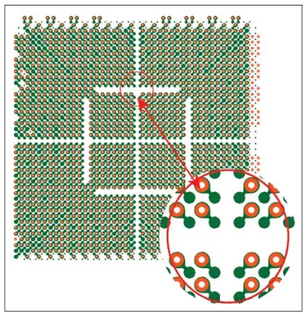
I. Characteristics of BGA Packaging and Its Impact on Wiring
BGA packaging differs significantly from peripheral lead packaging in that its solder joints are not easily accessible from the outer layer, especially for large-size, full-grid array BGA packages. Due to the dense arrangement of solder joints and the small spacing between connection pads, wiring space is limited. Therefore, designers need to fully consider how to effectively route signals from the bottom of the middle of the package.
II. Outgoing Wire Strategies
The outgoing wire strategy is a critical aspect of BGA packaging design. Designers need to select appropriate outgoing wire methods based on factors such as BGA package pitch, pin count, and PCB space layout. Here are some common outgoing wire strategies:
Using vias to route signals: For BGA packages with larger pitches and fewer pins, some pins can be directly routed through the outer layer. However, for most BGA packages, especially large-size, full-grid array packages, vias are needed to route signals from the bottom of the middle of the package. During design, it is necessary to ensure that the position, size, and number of vias meet wiring requirements.
Fan-out strategy: Fan-out is the process of evenly distributing BGA package pin signals onto the PCB. Successful fan-out strategies include aligning the layout grid with the fan-out grid, protecting BGA fan-out vias during wiring, and selecting appropriate via and pad sizes. Additionally, considering not fanning out the outermost two rows/columns of pins of the BGA can form a double-row inline package pattern, facilitating wiring for non-BGA nets.
III. Wiring Strategies
Wiring strategies directly affect the signal transmission performance and reliability of BGA packaging. When wiring, attention should be paid to the following points:
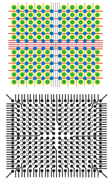
Power and ground lead placement: To facilitate wiring, power and ground leads can be placed in the center of the array pattern and directly connected to vias, avoiding interference with wiring on the outer edge of the package.
Selection of conductor width and spacing: Conductor width and spacing need to be determined based on factors such as BGA package pitch, pad size, and wiring space. While ensuring signal transmission performance, conductor width and spacing should be minimized as much as possible to increase wiring density.
Optimization of fan-out patterns: The fan-out pattern should display a unique cross shape for power to avoid power isolation. At the same time, the cross shape also leaves room for internal or crossed BGA network wiring.
Addressing the challenges of high-density wiring: As BGA package pitches decrease, more stringent shape control is required for PCB via patterns. Designers need to adopt smaller via pads and drilling sizes and reduce PCB layer count or dielectric thickness between layers to address the challenges of high-density wiring.
IV. Mechanical Strain Design
Mechanical strain and PCB bending are the main causes of damage to PCB and BGA solder joints. To reduce the impact of mechanical strain on BGA, designers need to take the following measures:
Rational layout of conductors and dogbones: Divide each BGA into four equal quadrants using lines parallel to the sides. Arrange conductors and dogbones within each quadrant to route from the BGA pad to the via, radiating at a 45-degree angle. This can increase the number of strains that the corner pads can withstand before damage.
Optimization of screw positions: Avoid placing screws along the BGA diagonal near the corner solder joints. Instead, preferably place screws or bosses at the midpoint of the BGA side. Additionally, using rigid bodies and plug connectors with PCA support at both ends can also reduce the impact of mechanical strain.
V. Internal Via Holes in Pads and Their Impact on Reliability
Internal via holes in BGA pads (plated-through holes, shielded on the reverse side of the PCB) can cause voids in BGA solder joints, potentially affecting reliability. However, for standard packages and BGA solder joints under specific design conditions, such voids do not necessarily lead to reliability issues. Designers need to assess the impact of internal via holes in pads on reliability based on specific application scenarios and environmental design standards.
VI. Micro-via Hole Strategy for Dense Pitch BGA Pads
For BGA full-array components with pitches less than 0.8mm, mechanical drilling technology cannot meet the hole placement requirements. To increase wiring area and density, a micro-via hole strategy is needed. These holes are typically formed by laser drilling and can connect blind holes in the first or second internal layer of the PCB. However, when using micro-via holes, attention should be paid to avoiding air entrapment and solder ball void issues.
VII. Power and Ground Connection Design
When connection pads are required within power or ground planes, access to the pads can be provided by leaving openings in the solder mask-covered plane. To increase fatigue life or thermal isolation, a crescent-shaped embossed pattern can be etched around the pad to create an MD pad. The MD segment should be arranged so that the SMD segment faces the corner of the BGA to provide maximum fatigue resistance.