 PCB
PCB FPC
FPC Rigid-Flex
 FR-4
FR-4 HDI PCB
 Rogers High-Frequency Board
 PTFE Teflon High-Frequency Board
 Aluminum
 Copper Core
 PCB Assembly
 LED light PCBA
 Memory PCBA
 Power Supply PCBA
 New Energey PCBA
 Communication PCBA
 Industrial Control PCBA
 Medical Equipment PCBA
 Testing Service
 PCBA Testing Service
 Certification Application
 RoHS Certification Application
 REACH Certification Application
 CE Certification Application
 FCC Certification Application
 CQC Certification Application
 UL Certification Application
 Transformers, Inductors
 High Frequency Transformers
 Low Frequency Transformers
 High Power Transformers
 Conversion Transformers
 Sealed Transformers
 Ring Transformers
 Inductors
 Wires,Cables Customized
 Network Cables
 Power Cords
 Antenna Cables
 Coaxial Cables
 Net Position Indicator
 Solar AIS net position indicator
 Capacitors
 Connectors
 Diodes
 Embedded Processors & Controllers
 Digital Signal Processors (DSP/DSC)
 Microcontrollers (MCU/MPU/SOC)
 Programmable Logic Device(CPLD/FPGA)
 Communication Modules/IoT
 Resistors
 Through Hole Resistors
 Resistor Networks, Arrays
 Potentiometers,Variable Resistors
 Aluminum Case,Porcelain Tube Resistance
 Current Sense Resistors,Shunt Resistors
 Switches
 Transistors
 Power Modules
 Isolated Power Modules
 AC-DC Power Modules
 DC-AC Module(Inverter)
 RF and Wireless
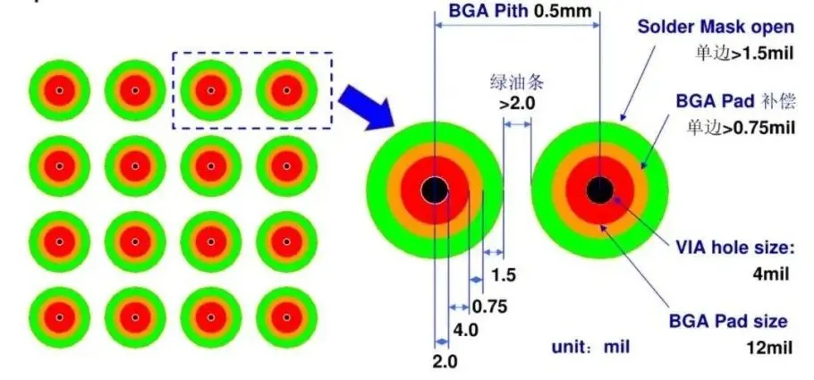
Optimal Pad Diameter-to-Ball Diameter Ratio for 0.3mm Ball Diameter, 0.5mm Pitch BGA Pads to Ensure Soldering Reliability
2025-11-13
Ball Grid Array (BGA) packages with a 0.3mm ball diameter and 0.5mm pitch are widely used in miniaturized, high-density electronic devices—such as smartphones, IoT Modules, and medical equipment—due to their compact footprint and high I/O density. The design of BGA pads is critical to soldering reliability, and the ratio of pad diameter to ball diameter (Dₚ/Dᵦ) is a core parameter that directly influences solder joint formation, mechanical strength, and long-term stability. This article details the optimal Dₚ/Dᵦ ratio range, underlying principles, influencing factors, and practical design guidelines based on industry standards (e.g., IPC-7351, IPC-A-610) and engineering validation data.
1. Core Principles: Why Dₚ/Dᵦ Ratio Matters for Soldering Reliability
The Dₚ/Dᵦ ratio governs the formation of a robust solder joint, which relies on balanced wetting, volume distribution, and mechanical resilience:
- Solder wetting and joint shape: A properly sized pad ensures the molten solder wets the pad fully without excessive spreading (which causes bridging between adjacent pads) or insufficient coverage (which leads to weak joints). The ideal solder joint forms a "fillet" with a contact angle of 30–60°, providing maximum adhesion between the BGA ball and pad.
- Mechanical strength: The solder joint must withstand thermal cycling, vibration, and mechanical stress during device operation. An optimal Dₚ/Dᵦ ratio ensures the joint has sufficient cross-sectional area to resist fatigue cracking (a common failure mode in BGA assemblies).
- Flux evacuation: During reflow soldering, flux must escape freely to prevent voids. The pad size, relative to the ball, influences the gap between the BGA package and PCB, affecting flux flow and void formation.
For a 0.3mm BGA ball (Dᵦ = 0.3mm) and 0.5mm pitch, the pad diameter (Dₚ) must balance these factors to avoid defects like bridging (due to overly large pads), insufficient solder coverage (overly small pads), or voids (poor flux evacuation).
2. Optimal Dₚ/Dᵦ Ratio Range
Based on extensive testing and industry consensus, the optimal Dₚ/Dᵦ ratio for 0.3mm ball diameter, 0.5mm pitch BGA pads is 0.6–0.8. Translating to actual pad diameters:
- Minimum Dₚ = 0.3mm × 0.6 = 0.18mm
- Maximum Dₚ = 0.3mm × 0.8 = 0.24mm
This range ensures soldering reliability across common manufacturing conditions. Below is a breakdown of peRFormance within and outside this range:
2.1 Ratio = 0.6–0.8 (Optimal Range)
- Solder joint quality: Molten solder forms a uniform fillet with 30–50° contact angle. Wetting is complete (100% pad coverage), and no bridging occurs between adjacent pads (thanks to the 0.5mm pitch, which provides 0.26mm minimum gap between 0.24mm maximum pads).
- Mechanical reliability: Solder joints withstand 1000+ thermal cycles (-40°C to 125°C) without cracking. Shear strength tests show joints can resist 8–12N of force (exceeding the IPC-6012 requirement of ≥5N for fine-pitch BGAs).
- Void rate: Voids account for <5% of the solder joint volume (within the IPC-A-610 acceptable limit of ≤10%), as flux evacuates effectively through the gap between the BGA package and PCB.
2.2 Ratio < 0.6 (Undersized Pads)
- A ratio of 0.5 (Dₚ = 0.15mm) leads to insufficient solder wetting—pad coverage drops to 70–80%, forming irregular fillets with contact angles >70°.
- Shear strength decreases to 3–5N, making joints prone to failure under thermal cycling or vibration.
- Voids increase to 15–20% of joint volume, as flux is trapped between the ball and undersized pad.
2.3 Ratio > 0.8 (Oversized Pads)
- A ratio of 0.9 (Dₚ = 0.27mm) creates a high risk of bridging between adjacent pads. The gap between pads shrinks to 0.23mm, and molten solder can spread across the gap (especially with excessive solder paste).
- Solder joints become "bulky" with uneven fillets, leading to stress concentration at the pad edges. Thermal cycling tests show cracking after 500–800 cycles.
- The large pad size reduces the gap between BGA and PCB, hindering flux evacuation and increasing void formation in some cases.
3. Factors Adjusting the Optimal Ratio
While 0.6–0.8 is the baseline optimal range, it can be adjusted slightly based on three key design and manufacturing factors:
3.1 Solder Paste Type and Application
- Type 4 solder paste (particle size 20–38μm) is ideal for fine-pitch BGAs. It allows a slightly lower ratio (0.55–0.75) due to better printability and controlled solder spread.
- Type 3 solder paste (38–75μm particles) requires a higher ratio (0.65–0.85) to compensate for larger particle size and potential uneven spreading.
- Solder paste volume: Applying 10–15% more paste (e.g., via a 0.12mm stencil aperture) allows a lower ratio (0.55–0.7) without compromising coverage.
3.2 PCB Manufacturing Tolerances
- PCBs with tight pad diameter tolerance (±0.01mm) can use the full 0.6–0.8 range. For PCBs with looser tolerance (±0.02mm), the ratio should be narrowed to 0.65–0.75 to avoid drifting outside the effective range.
- Pad finish: ENIG (Electroless Nickel Immersion Gold) finish has better solder wetting than OSP (Organic Solderability Preservative), allowing a 5–10% lower ratio while maintaining reliability.
3.3 BGA Package Variations
- Package coplanarity: BGAs with excellent coplanarity (≤0.03mm) can use the lower end of the ratio (0.6–0.7), as uniform contact between balls and pads ensures consistent wetting.
- Ball oxidation: BGAs with minimal ball oxidation (common in vacuum-packaged components) allow a slightly lower ratio (0.55–0.75). Oxidized balls require a higher ratio (0.65–0.85) to ensure sufficient wetting.
4. Practical Design Guidelines
To maximize soldering reliability for 0.3mm ball, 0.5mm pitch BGAs, follow these industry best practices:
- Set the pad diameter to 0.20–0.22mm (Dₚ/Dᵦ = 0.67–0.73) as a "safe middle ground" within the optimal range. This balances wetting, anti-bridging, and mechanical strength for most manufacturing scenarios.
- Use non-solder mask defined (NSMD) pads instead of solder mask defined (SMD) pads. NSMD pads have better solder joint formation and mechanical strength, as the solder mask does not restrict pad edges.
- Maintain a solder mask opening (SMO) 0.02–0.03mm larger than the pad diameter (e.g., 0.22–0.25mm SMO for a 0.20mm pad). This prevents solder mask from interfering with wetting.
- For high-reliability applications (e.g., automotive, aerospace), narrow the ratio to 0.65–0.75 (Dₚ = 0.195–0.225mm) and use Type 4 solder paste with ENIG pad finish.
5. Validation Methods for Ratio Suitability
Before mass production, validate the chosen Dₚ/Dᵦ ratio using these tests:
- Solder joint inspection: Use X-ray imaging to check for voids (<10% volume) and bridging (no adjacent pad connection).
- Shear strength testing: Verify joints can withstand ≥5N of shear force (per IPC-6012).
- Thermal cycling test: Subject assemblies to 1000 cycles of -40°C to 125°C (15-minute dwell time) and check for joint cracking via X-ray or cross-sectional analysis.
For BGA pads with a 0.3mm ball diameter and 0.5mm pitch, the optimal pad diameter-to-ball diameter ratio (Dₚ/Dᵦ) is 0.6–0.8 (corresponding to a pad diameter of 0.18–0.24mm). This range ensures proper solder wetting, avoids bridging, minimizes voids, and provides sufficient mechanical strength for long-term reliability. Adjustments to the range (±0.05) can be made based on solder paste type, PCB manufacturing tolerances, and BGA package characteristics. By adhering to this ratio and following practical design guidelines, engineers can achieve consistent, reliable BGA soldering in high-density electronic devices.