 PCB
PCB FPC
FPC Rigid-Flex
 FR-4
FR-4 HDI PCB
 Rogers High-Frequency Board
 PTFE Teflon High-Frequency Board
 Aluminum
 Copper Core
 PCB Assembly
 LED light PCBA
 Memory PCBA
 Power Supply PCBA
 New Energey PCBA
 Communication PCBA
 Industrial Control PCBA
 Medical Equipment PCBA
 Testing Service
 PCBA Testing Service
 Certification Application
 RoHS Certification Application
 REACH Certification Application
 CE Certification Application
 FCC Certification Application
 CQC Certification Application
 UL Certification Application
 Transformers, Inductors
 High Frequency Transformers
 Low Frequency Transformers
 High Power Transformers
 Conversion Transformers
 Sealed Transformers
 Ring Transformers
 Inductors
 Wires,Cables Customized
 Network Cables
 Power Cords
 Antenna Cables
 Coaxial Cables
 Net Position Indicator
 Solar AIS net position indicator
 Capacitors
 Connectors
 Diodes
 Embedded Processors & Controllers
 Digital Signal Processors (DSP/DSC)
 Microcontrollers (MCU/MPU/SOC)
 Programmable Logic Device(CPLD/FPGA)
 Communication Modules/IoT
 Resistors
 Through Hole Resistors
 Resistor Networks, Arrays
 Potentiometers,Variable Resistors
 Aluminum Case,Porcelain Tube Resistance
 Current Sense Resistors,Shunt Resistors
 Switches
 Transistors
 Power Modules
 Isolated Power Modules
 AC-DC Power Modules
 DC-AC Module(Inverter)
 RF and Wireless
Core Principles and Practical Tips for PCB Routing
2025-11-26
1. Prioritize Manual Routing
Modern Pcb Design software includes auto-routing features, but no auto-routing tool can replace an engineer’s experience and flexibility. Auto-routing is only recommended for these scenarios:
- After component placement, use auto-routing to check the "completion rate": if it’s below 85%, your component layout needs adjustment;
- Identify routing bottlenecks: use auto-routing to quICkly locate potential obstacles at critical connection points;
- Inspiration reference: when stuck on routing ideas, use auto-routing to generate a preliminary plan as a reference.
The precision, signal integrity, and reliability of routing ultimately depend on manual control, so manual routing is recommended for core areas.
2. Clarify Manufacturer’s Process Specifications in Advance
Before starting routing, confirm these key parameters with your PCB manufacturer:
- Minimum line width and spacing requirements;
- Maximum supported PCB layer count;
- Manufacturing tolerances for pads and vias.
Presetting these parameters as design rules (e.g., line width/spacing thresholds) avoids re-routing later due to process incompatibility, significantly improving design efficiency.
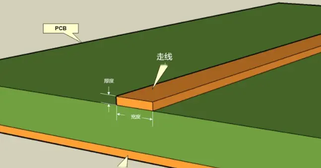
3. Match Trace Width to Current Requirements
Trace width must align with the current it carries:
- Calculate minimum line width: Determine the minimum width based on current (combined with copper thickness and ambient temperature) to avoid overheating from excessive current;
- Widen traces when space allows: If PCB space is sufficient, use a width larger than the minimum to enhance thermal management;
- Advantage of outer-layer traces: Outer-layer traces directly contact air, so they have higher heat exchange efficiency and can be slightly narrowed for the same current.
4. Maintain Safe Spacing Between Traces and Pads
Adequate gaps between traces, pads, and adjacent traces are critical to avoid short circuits during manufacturing or assembly. Generally:
- The gap between adjacent traces/pads should not be smaller than the manufacturer’s minimum line spacing;
- Gaps for sensitive signals (e.g., high-voltage, high-frequency) should be enlarged by 20-30% to prevent creepage or crosstalk.
5. Strategically Plan Component Placement
Component placement is the foundation of successful PCB design. Follow these rules:
- Separate heat-sensitive and heat-generating components: Keep heat-sensitive components (e.g., electrolytic capacitors) away from heat sources (e.g., Diodes, inductors);
- Prioritize multi-pin components: Components like BGAs or QFPs occupy large space and require early layout planning;
- Unify component orientation: Align similar components (e.g., resistors, capacitors) in the same direction for easier soldering and maintenance;
- Physical pre-verification: If components are already procured, print a 1:1 layout to check if their physical dimensions fit.
6. Isolate Analog and Digital Traces
Digital signals (especially high-frequency ones) easily generate electromagnetic interference and must be physically isolated from analog traces:
- Avoid parallel routing of high-frequency digital traces (e.g., data buses) with analog traces to prevent capacitive coupling;
- If PCB space is limited, separate analog and digital areas with a ground plane to block interference paths.
7. Design the Ground Plane Properly
At least one complete ground plane is required (instead of scattered ground traces):
- A full ground plane provides a unified voltage reference for all signals, avoiding resistance/voltage drop differences from scattered grounding;
- In multi-layer boards, place the ground and power planes in inner layers and keep them symmetric to enhance noise immunity and prevent PCB warping;
- Placing a ground plane under signal traces reduces trace impedance and suppresses crosstalk.
8. Reserve Safe Space Around Mounting Holes
Mounting holes need a "component/trace-free zone" around them:
- Reserve at least 1mm of empty space beyond the physical size of the mounting hole;
- Do not rely on solder mask as the only insulator—spatial isolation is necessary to avoid electrical shock risks.
9. Alternate Trace Directions Between Layers
To reduce inter-layer crosstalk, route adjacent layers in perpendicular directions:
- If one layer uses primarily horizontal traces, the adjacent layer should use vertical traces;
- Short, straight traces are preferred—avoid excessive path lengthening when routing around obstacles.
10. Techniques to Suppress Capacitive Coupling
Capacitive coupling is a major source of high-frequency signal interference. Mitigate it with:
- Assign dedicated layers to power and analog signal traces to avoid overlapping with ground planes;
- Keep decoupling capacitor traces as short as possible and place them close to component power terminals to compensate for component capacitive loads;
- Shorten long parallel trace segments or insert ground vias between them to block coupling paths.
11. Optimize Thermal Vias and Thermal Pads
Thermal management is critical for high-power PCBs. Arrange thermal structures properly:
- Add thermal pads under through-hole components to simplify soldering and improve heat dissipation;
- Place multiple thermal vias under power components (e.g., ICs) to transfer heat from inner layers to outer layers or heat sinks;
- Thermal vias should serve both "electrical connection" and "heat conduction"—use large diameters (e.g., 0.5mm) and dense arrangements.
12. Widen Power and Ground Traces
Power and ground traces carry larger currents, so:
- Their width should be significantly larger than signal traces (common rule: power/ground width ≥ 0.040 inches, signal trace width ≥ 0.025 inches);
- Wider power/ground traces reduce overcurrent risks and are easier to identify visually, minimizing wiring errors;
- For high-current power supplies, replace traces with copper pours to further enhance current-carrying capacity.
13. Use the Silkscreen Layer Efficiently
The silkscreen layer marks key information, but keep it concise and practical:
- Avoid excessive text that wastes space—there’s no need to label minor parameters like resistor values;
- Use moderate text size (≥1.27mm recommended) to ensure clarity when printed;
- Do not print text on exposed copper pads, as ink can block solder flow and cause cold solder joints.
14. Avoid 90° Trace Corners
90° or sharp corners cause two main issues:
- Impaired high-frequency signal integrity: Right angles create impedance discontinuities, increasing crosstalk, radiation, and signal reflection;
- Manufacturing risks: 90° outer corners are prone to over-etching, leading to narrowed traces or short circuits.
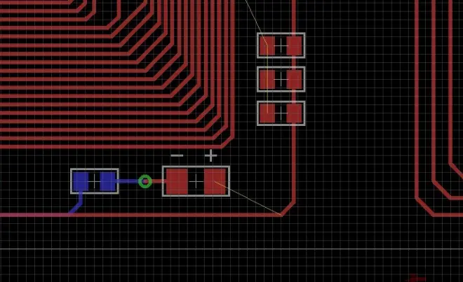
Replace 90° corners with two 45° angles or rounded transitions to balance routing efficiency and signal quality.