 PCB
PCB FPC
FPC Rigid-Flex
 FR-4
FR-4 HDI PCB
 Rogers High-Frequency Board
 PTFE Teflon High-Frequency Board
 Aluminum
 Copper Core
 PCB Assembly
 LED light PCBA
 Memory PCBA
 Power Supply PCBA
 New Energey PCBA
 Communication PCBA
 Industrial Control PCBA
 Medical Equipment PCBA
 Testing Service
 PCBA Testing Service
 Certification Application
 RoHS Certification Application
 REACH Certification Application
 CE Certification Application
 FCC Certification Application
 CQC Certification Application
 UL Certification Application
 Transformers, Inductors
 High Frequency Transformers
 Low Frequency Transformers
 High Power Transformers
 Conversion Transformers
 Sealed Transformers
 Ring Transformers
 Inductors
 Wires,Cables Customized
 Network Cables
 Power Cords
 Antenna Cables
 Coaxial Cables
 Net Position Indicator
 Solar AIS net position indicator
 Capacitors
 Connectors
 Diodes
 Embedded Processors & Controllers
 Digital Signal Processors (DSP/DSC)
 Microcontrollers (MCU/MPU/SOC)
 Programmable Logic Device(CPLD/FPGA)
 Communication Modules/IoT
 Resistors
 Through Hole Resistors
 Resistor Networks, Arrays
 Potentiometers,Variable Resistors
 Aluminum Case,Porcelain Tube Resistance
 Current Sense Resistors,Shunt Resistors
 Switches
 Transistors
 Power Modules
 Isolated Power Modules
 AC-DC Power Modules
 DC-AC Module(Inverter)
 RF and Wireless
Fanout Routing Principles for Low-Speed IC Pins (e.g., MCU): A Comprehensive Analysis
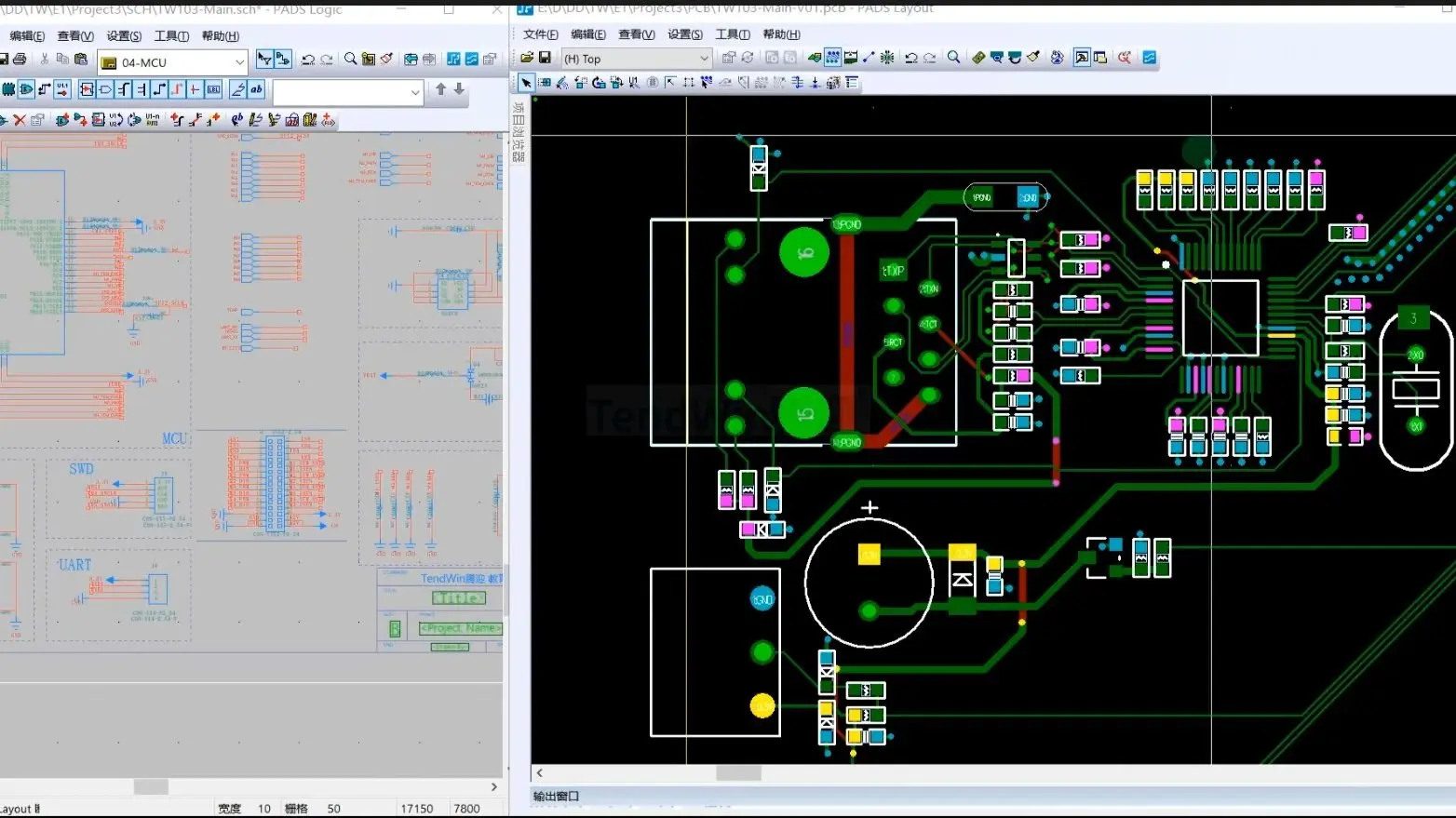
Abstract: Fanout routing for low-speed IC pins aims to balance manufacturability, testability, and signal integrity. Per IPC-2221 and device manuals, core principles include power layer planning, shortest path, teardrop transitions, and test point allocation, ensuring compliance with 3W rule (spacing ≥3× line width) and 10° routing angle.
1. Power & Ground Handling
-
Decoupling Capacitor Priority:
-
Place 0.1μF cap per VDD/GND pair within ≤1.5mm (Cap→Pin→IC path <2.5mm).
-
Add 10μF bulk capacitor at power entry (≤5mm from IC).
-
-
Stackup Strategy:
-
4-layer: Solid L2 (GND) and L3 (VCC) planes;
-
2-layer: Power/GND trace width ≥0.5mm with grid copper (grid spacing 2–3mm).
-
2. Signal Routing Standards
-
Path Optimization:
-
Minimize Length: Trace length ≤3× pin pitch (e.g., 0.5mm pitch IC → ≤15mm);
-
No 90° Angles: Use 45° or arcs (radius ≥1.5× width) to reduce impedance discontinuity.
-
-
Spacing Control:
Parameter Standard Value High-Density Limit Trace Width (W) 0.2–0.3mm (8–12mil) 0.15mm (6mil) Trace Spacing (S) ≥3W (≥0.6mm) ≥2W (≥0.3mm) Pad Exit Distance (D) 0.2mm (8mil) 0.1mm (4mil) -
Teardrop Transition:
-
Add teardrops at pad-trace junctions (width taper ratio 0.6) to reduce stress (IPC-2221 9.1.1).
-
3. Design for Manufacturability (DFM)
-
Via Strategy:
-
Via hole ≥0.2mm (8mil), pad ≥0.4mm (16mil);
-
No vias under pads (keepout ≥0.15mm from pad edge).
-
-
Test Point Allocation:
-
Add 1.0mm-dia test pads for critical nets (reset, clock), ≥2mm from IC body;
-
Test point coverage ≥90% (flying probe requirement).
-
-
SilkSCReen Marking:
-
Pin 1 marker ≥0.2mm from pad; character height ≥1.0mm.
-
4. Special Signal Handling
-
Reset/Clock Traces:
-
Guard traces: Add GND shields on both sides (spacing 2W);
-
Length matching: Intra-group length mismatch ≤5mm.
-
-
Unused Pins:
-
Configured as output: Leave floating with test point;
-
Configured as input: Pull up/down to VCC/GND (10kΩ resistor).
-
5. Verification & Optimization
-
DRC Rule Settings:
Clearance: 0.2mm (signal), 0.3mm (power) Via to Trace: 0.15mm Min. Hole Size: 0.2mm -
Simulation:
-
SPICE: Check signal ringing (overshoot <15% VDD);
-
IR Drop Analysis: Voltage drop <3% (at full load).
-
Conclusion
Low-speed IC fanout follows "Three Priorities":
-
Power Integrity: Decoupling caps adjacent to pins (≤1.5mm); solid reference planes;
-
Manufacturability: Teardrops + 3W spacing + 45° routing;
-
Testability: 100% test point coverage for critical nets.
Design Redline: Avoid "dog-bone" fanout in BGA areas (unless Via-in-Pad); use "direct drill" or "VIPPO" technology.