 PCB
PCB FPC
FPC Rigid-Flex
 FR-4
FR-4 HDI PCB
 Rogers High-Frequency Board
 PTFE Teflon High-Frequency Board
 Aluminum
 Copper Core
 PCB Assembly
 LED light PCBA
 Memory PCBA
 Power Supply PCBA
 New Energey PCBA
 Communication PCBA
 Industrial Control PCBA
 Medical Equipment PCBA
 Testing Service
 PCBA Testing Service
 Certification Application
 RoHS Certification Application
 REACH Certification Application
 CE Certification Application
 FCC Certification Application
 CQC Certification Application
 UL Certification Application
 Transformers, Inductors
 High Frequency Transformers
 Low Frequency Transformers
 High Power Transformers
 Conversion Transformers
 Sealed Transformers
 Ring Transformers
 Inductors
 Wires,Cables Customized
 Network Cables
 Power Cords
 Antenna Cables
 Coaxial Cables
 Net Position Indicator
 Solar AIS net position indicator
 Capacitors
 Connectors
 Diodes
 Embedded Processors & Controllers
 Digital Signal Processors (DSP/DSC)
 Microcontrollers (MCU/MPU/SOC)
 Programmable Logic Device(CPLD/FPGA)
 Communication Modules/IoT
 Resistors
 Through Hole Resistors
 Resistor Networks, Arrays
 Potentiometers,Variable Resistors
 Aluminum Case,Porcelain Tube Resistance
 Current Sense Resistors,Shunt Resistors
 Switches
 Transistors
 Power Modules
 Isolated Power Modules
 AC-DC Power Modules
 DC-AC Module(Inverter)
 RF and Wireless
How to design high-quality wave soldering tooling fixtures? What are the key points?
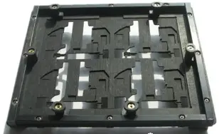
1、Ensure the flatness of the PCB to prevent deformation and bending. The fixture should be made of high-temperature-resistant materials so that it is not easy to deform at the soldering temperature.
2、Protect the suRFace-mounted components and enable them to pass through the wave soldering safely. The fixture can protect the components from the thermal shock of the wave and prevent the soldering joints from being misaligned.
3、Improve production efficiency. Using the fixture can pass a larger number of Pcb Boards at one time, reducing the production time.
4、Optimize the design for easy operation. The design of the fixture should be simple and easy to use, making it convenient for employees to get started and reducing the operation difficulty.
1、Determine the material and specification of the fixture. According to the production needs, select the appropriate material and specification to meet the requirements of high temperature resistance, high strength, etc.
2、Design a reasonable structure. The structure of the fixture should be reasonable and able to meet various needs in the production process, such as fixing the PCB and protecting the components.
3、Determine the positioning method. The fixture should be able to accurately position the PCB to ensure the soldering effect and quality. Common positioning methods include hole positioning, edge positioning, etc.
4、Consider the heat dissipation problem. Since the fixture needs to withstand a high-temperature environment, the heat dissipation problem needs to be fully considered to prevent the performance from decreasing or being damaged due to excessive temperature.
5、Easy to clean and maintain. After the fixture is used for a period of time, it needs to be cleaned and maintained to maintain its performance and accuracy. Therefore, the characteristics of being easy to clean and maintain should be considered in the design to improve production efficiency.
In short, the design of wave soldering fixtures needs to be specifically analyzed and designed in combination with the actual production needs to ensure that it is suitable for the production environment and improves production efficiency and product quality.
1、A clearance width of 0.5mm (bilateral) should be reserved for the cooperation between the edge of the PCB board and the fixture to prevent the PCB board from deforming due to thermal expansion when passing through the soldering furnace, resulting in poor soldering. The tolerance is usually ±0.1mm.
2、The sinking depth of the fixture is 1.5mm, and its tolerance is ±0.1mm.
3、For the components on the PCB board that need to be tinned and have holes, considering factors such as the balance and height of the tin wave flow, for the insertion holes in the non-tin-passing direction, the distance between the component leads and the hole edge on both sides is ≥ 3mm; in the tin-passing direction, to avoid the shadow effect, it is necessary to ensure that the distance between the component leads and the hole edge (single side) is ≥ 5mm. Please refer to the following attached drawings for details:
4、To avoid poor soldering of components and reduce short circuits, at the opening of the fixture, in order to reduce the adverse impact of the shadow effect on soldering, the reverse side of the fixture must be chamfered. The chamfer angle should be as large as possible, but the remaining thickness after chamfering should be ≥ 0.8mm. Usually, the chamfer angle is 25°±5°, and the chamfer depth is 1.5mm±0.1mm, as shown in the figure: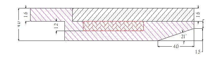
5、For the BGA on the PCB board, special protection must be provided when designing the fixture to prevent the BGA components from being damaged by high temperature when passing through the soldering furnace. Therefore, a clearance of 1.2mm~1.5mm must be left at the position of the BGA, and the minimum remaining board thickness after sinking should be more than 1.0mm.
6、The pressing blocks and tin-blocking strips on the fixture must be chamfered. The material of the pressing blocks must be resistant to high temperature. Usually, imported red and black bakelite boards are used. The contact distance between the pressing blocks and the edge of the PCB board is 3~4mm, and try to avoid the components on the PCB board to prevent scratching and damaging the components.
7、In order to improve the service life of the fixture and prevent the components from being damaged by static electricity, the fixture must be made of black anti-static synthetic stone material. The specific material shall be subject to the production order.
8、The thickness of the synthetic stone:
6mm: For the fixtures of models with a carrier width of less than 420mm (except for special cases)
8mm: In special cases such as when the SMT components at the bottom of the board are too large, special metal accessories are installed on the fixture, and the fixture has a sunken connecting strip, etc.; for double-sided boards with a carrier width of more than 420mm, an aluminum alloy frame and an aluminum alloy tin-proof strip need to be added at the same time.
Patching rules: Try to avoid using patches. Considering the height of the components at the bottom of the board, if the 8mm material can be used without adding patches, choose the 8mm thickness material.
9、Generally, a snap is distributed every about 8cm, and the rotation path of the snap should avoid the SMT components. A Gap of about 1mm is required to be reserved. In necessary cases, consider installing a fool-proof post to ensure that the snap can only rotate at a certain angle. The shrapnel is set according to the distribution of DIMM and PCI. If there are special requirements, make special instructions on the production order.
10、To ensure that the fixture can smoothly pass through the nozzle of the core of the soldering furnace, the bottom of the fixture must be kept flat. Therefore, the countersink depth of the reverse side of the screw must be greater than the thickness of the screw head, and the metal material at the bottom of the carrier cannot be contaminated with tin.
11、In order to make the fixture fit well with the track of the soldering furnace and improve the soldering performance, the thickness of the bearing edge of the fixture is set to 4+2mm to achieve the coplanarity effect. The width of the left and right tracks is 7mm each to achieve the best parallel performance, and the tolerance is between ±0.1mm. For the carriers with patches exceeding 6mm at the bottom, the design of the bearing edge is as shown in the following figure.
12、Metal reinforcing ribs must be set for DIMM openings with more than 8 pins.
13、Holes larger than Φ2mm that are not for inserting components must be blocked. If it cannot be achieved, it should be specified in the design.
14、The manufacturer is responsible for the design of the integrated pressure cover. The design verification should be evaluated from the trial production stage, and it should be synchronously introduced during mass production. It should be noted that the height of the carrier after the design is completed should not exceed 30mm (excluding patches).
15、Before the soldering furnace fixture is put into use, the relevant information such as the part number version of the fixture, the direction of passing through the soldering furnace, and the serial number of the fixture must be marked according to the relevant definitions of IE. The engraving specifications uniformly use Arial font size 22 for English and FangSong font size 22 for Chinese.
16、The carrier is equipped with a bar code. The size of the bar code is provided by MSL. The material is required to be 1mm thick aluminum alloy with anodized blackening treatment. The manufacturer should reserve installation holes when designing the carrier, and the installation position should avoid the travel of all shrapnels.
17、The locking plate nuts and positioning posts are set according to the actual situation for the screw holes. After the locking plate nuts are installed, they must sink 0.5mm. The specific parameters are shown in the following figure. And it is required that there is no risk of collision between the locking plate studs and any components on the PCB board during the locking process (the distance from the center of the nut to the surrounding components is not less than 5.5mm, that is, the Gap is not less than 1.5mm).
18、Requirements for flatness: All processed surfaces must be ensured to be flat. Inspection method: Place the bottom surface on a marble surface to observe whether there is warping of the board. For other processed surfaces, first ensure that there is no obvious warping of the board through visual inspection, and then use tools (vernier calipers, 3D tester, etc.) to measure. The specific inspection parameters are detailed in the "Inspection and Acceptance Record Form for Soldering Furnace Fixtures".
19、"Tin Stealing Technology Design": In order to reduce the occurrence of bridging between the pins at the tail end of the connector during soldering, the "tin stealing technology design" for the soldering furnace fixture can be considered. Install tin stripping pieces at the same pitch distance behind the pins with bridging at the tail end on the soldering furnace fixture, and connect them firmly to the soldering furnace fixture with screws or rivets. It is made of metal materials with a low melting rate, and the thickness is 1.0~2.0mm; the end of the tin stripping piece close to the pin should be chamfered, and the thickness of the end part is preferably 0.5mm to achieve the effect of eliminating bridging. The span of the tin stripping piece should not be too large. After it is fixed to the soldering furnace fixture, it must be ensured that its upper surface can be in close contact with the bottom surface of the PCBA board to avoid damaging the PCBA due to the overflow of tin when passing through the wave soldering furnace.
Note: The "tin stealing design" of the soldering furnace fixture should be avoided as much as possible and should be used only when adjusting the wave soldering furnace cannot solve the problem of tin coating and bridging.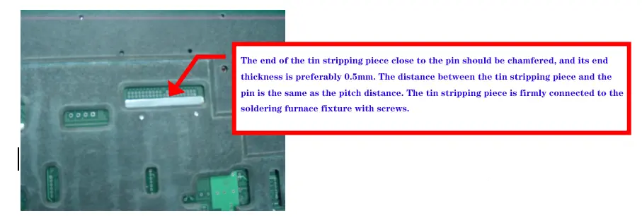
20、The manufacturer is required to provide the film and acrylic. The requirements for the film and acrylic are as follows:
Film: The film is color-printed, and the PAD of the SMT components at the bottom of the board and the silk-screened wire frame are in different colors respectively; the component leads on the board surface are black.
Acrylic: The specification of the acrylic should be the same as the sinking range of the board; both the acrylic and the film should have through holes at the corresponding positions of the positioning posts (simulate the board to check the fixture);
21、All locking plate nuts need to be equipped with screws. The specific screw specifications are as follows:
For board thickness less than 3mm, the top of the screw is with a cylindrical step.
For board thickness greater than or equal to 3mm, the top of the screw is conical.
22、When the width of the carrier is greater than or equal to 440mm, aluminum alloy strips need to be used in the width direction to increase the anti-deformation degree of the carrier. The height around the carrier needs to exceed 15mm. If it is less than 15mm, use synthetic stone strips to make up for it.
23、DIMM area opening principle: On the basis of the original opening range of the DIMM, add 3 semi-circular through holes with R10 on the left and right sides, so that the distance from the outermost DIMM pin to the center of the arc is not less than 15mm.
Installation precautions for the distance between the accessories and the DIMM:
Plan 1: The distance between each accessory installed on the side of the fixture and the center of the outermost DIMM is not less than 20mm;
Plan 2: Each accessory installed on the side of the fixture is outside the 30mm area of the center of the outermost DIMM.
24、Apply AB glue to all the places around the patches of all fixtures where glue can be applied to seal the patches and the main body of the fixture; also apply glue to the bottom of the screw holes for fixing the patches to prevent tin from remaining in the holes and generating tin tips.
25、After the drawings are verified and approved, they should be input into the server for archiving.