 PCB
PCB FPC
FPC Rigid-Flex
 FR-4
FR-4 HDI PCB
 Rogers High-Frequency Board
 PTFE Teflon High-Frequency Board
 Aluminum
 Copper Core
 PCB Assembly
 LED light PCBA
 Memory PCBA
 Power Supply PCBA
 New Energey PCBA
 Communication PCBA
 Industrial Control PCBA
 Medical Equipment PCBA
 Testing Service
 PCBA Testing Service
 Certification Application
 RoHS Certification Application
 REACH Certification Application
 CE Certification Application
 FCC Certification Application
 CQC Certification Application
 UL Certification Application
 Transformers, Inductors
 High Frequency Transformers
 Low Frequency Transformers
 High Power Transformers
 Conversion Transformers
 Sealed Transformers
 Ring Transformers
 Inductors
 Wires,Cables Customized
 Network Cables
 Power Cords
 Antenna Cables
 Coaxial Cables
 Net Position Indicator
 Solar AIS net position indicator
 Capacitors
 Connectors
 Diodes
 Embedded Processors & Controllers
 Digital Signal Processors (DSP/DSC)
 Microcontrollers (MCU/MPU/SOC)
 Programmable Logic Device(CPLD/FPGA)
 Communication Modules/IoT
 Resistors
 Through Hole Resistors
 Resistor Networks, Arrays
 Potentiometers,Variable Resistors
 Aluminum Case,Porcelain Tube Resistance
 Current Sense Resistors,Shunt Resistors
 Switches
 Transistors
 Power Modules
 Isolated Power Modules
 AC-DC Power Modules
 DC-AC Module(Inverter)
 RF and Wireless
Root Cause Analysis of Local Line Width Narrowing (Non-Open Circuit) in Inner-Layer PCB Traces Detected by AOI After Etching
2025-12-21
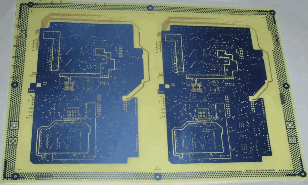
In printed Circuit Board (PCB) manufacturing, inner-layer trace etching is a critical subtractive process that defines the conductive pathways for signal transmission and power distribution in multi-layer boards. Automated Optical Inspection (AOI) systems play a pivotal role in verifying trace integrity post-etching, detecting defects such as line width deviations, shorts, opens, and undercuts. A common non-critical yet quality-concerning defect identified by AOI is local line width narrowing—a condition where specific segments of inner-layer traces are thinner than the design specification (typically by 10–30% of the nominal width) without forming a complete open circuit. This defect poses latent risks to PCB reliability: narrowed traces exhibit higher resistance, increased current density, and reduced thermal dissipation capacity, which can lead to signal attenuation, overheating, or even delayed open-circuit failures under long-term thermal cycling or mechanical stress.
For high-reliability applications (e.g., aerospace, automotive, medical devices), even minor line width narrowing violates IPC-6012 Class 3 standards, which mandate that inner-layer trace widths must deviate by no more than ±10% of the nominal value. To address this defect, a systematic root cause analysis is essential, as the issue stems from a combination of process variations, material inconsistencies, and equipment misalignments across the pre-etch, etching, and post-etch workflows. This article provides a comprehensive analysis of the potential causes of local line width narrowing in inner-layer traces, categorized by process stage, and correlates each cause with AOI defect characteristics to facilitate targeted troubleshooting.
1. Pre-Etching Process Deficiencies: The Foundation of Local Line Width Deviations
The pre-etching stage encompasses inner-layer lamination, photoresist coating, exposure, and development—processes that directly determine the pattern accuracy of the copper traces before etching. Any inconsistency in these steps can create latent pattern defects that manifest as line width narrowing during etching.
1.1 Uneven Photoresist Coating and Thickness Variations
Photoresist (PR) is a light-sensitive polymer that acts as a protective mask during etching: exposed PR areas are removed (for positive-tone PR) or retained (for negative-tone PR), leaving the underlying copper to be etched or protected. Uneven PR coating is a primary cause of local line width narrowing, driven by the following factors:
- Coating Equipment Calibration Errors: Inner-layer PCBs are typically coated with PR using spin-coating or curtain-coating machines. If the spin-coater’s rotational speed is inconsistent across the PCB suRFace, or if the curtain-coater’s nozzle has partial blockages, the PR layer will exhibit thickness gradients. Thinner PR regions (below the specified 1.5–2.5μm for inner layers) are more susceptible to over-exposure or developer penetration, leading to narrower PR masks.
- Substrate Surface Irregularities: Inner-layer cores (e.g., FR-4, polyimide) with uneven surface roughness (Ra > 0.8μm) or residual contaminants (e.g., dust, lint, lamination adhesive residues) cause PR to pool in low areas and thin out in high areas. On raised substrate regions, the PR mask is too thin to fully protect the copper during etching, resulting in local trace narrowing.
- PR Viscosity Fluctuations: Photoresist viscosity is temperature-dependent; deviations from the optimal range (200–300 cP for liquid PR) lead to uneven flow during coating. High-viscosity PR coats thicker and more unevenly, while low-viscosity PR spreads too thinly, especially on substrate edges or raised features.
AOI defect characteristics associated with PR thickness variations: Narrowed trace segments correspond to localized thin PR areas, often appearing as linear or patchy deviations aligned with substrate surface irregularities. The defect is typically non-uniform across the PCB, with more severe narrowing in regions where PR thickness is below the lower specification limit.
1.2 Photolithography Exposure Misalignment and Energy Non-Uniformity
Photolithography exposure transfers the trace pattern from a photomask to the PR-coated inner-layer core. Exposure-related errors are a leading cause of local line width narrowing, particularly for fine-pitch inner-layer traces (≤50μm width/spacing):
- Mask-to-Substrate Misalignment: The photomask and inner-layer core must be perfectly aligned during exposure to ensure that the PR pattern matches the design specifications. Even minor misalignment (≥5μm) can cause the PR mask to shift relative to the copper layer, resulting in narrower trace segments on one side of the pattern. This is common in step-and-repeat exposure systems with worn alignment pins or faulty vacuum chucks that fail to hold the substrate flat.
- Exposure Energy Gradients: Exposure lamps (e.g., mercury vapor lamps) exhibit non-uniform light intensity across their emission area, creating energy gradients on the PCB surface. High-energy regions over-expose the PR, causing the PR mask to shrink (for positive-tone PR) and narrow the trace width. Conversely, low-energy regions under-expose the PR, leading to under-development, but this typically causes line width broadening rather than narrowing.
- Photomask Defects: The photomask itself may have localized defects such as pinholes, scratches, or chrome plating wear. These defects allow extra light to reach the PR, creating smaller PR mask openings that translate to narrower copper traces after etching. For example, a 10μm scratch on the photomask chrome layer can cause a corresponding 10μm-wide narrowed segment on the inner-layer trace.
AOI defect characteristics associated with exposure errors: Narrowed traces often exhibit edge roughness or "tapered" edges, with the narrowing severity correlating to the exposure energy level. Mask misalignment-induced narrowing is typically directional (e.g., all narrowed segments are on the left edge of the trace), while photomask defects cause isolated, repeatable narrowing patterns across multiple PCBs processed with the same mask.
1.3 Developer Process Parameters and Contamination
The development stage removes the exposed PR (for positive-tone systems) to reveal the copper areas to be etched. Improper development can erode the PR mask edges, leading to local line width narrowing:
- Developer Concentration and Temperature Deviations: Developers (e.g., sodium carbonate solutions for positive-tone PR) must be maintained at a specific concentration (1–2%) and temperature (25–30°C). High developer concentration or temperature accelerates PR dissolution, causing the PR mask edges to erode and narrow the trace pattern. This effect is exacerbated in localized areas where the PR is already thin due to coating errors.
- Developer Agitation Non-Uniformity: Inadequate agitation (e.g., stagnant developer in spray nozzles) creates concentration gradients in the developer bath, with higher chemical activity in regions with fresh developer flow. These regions erode the PR mask more aggressively, leading to localized trace narrowing.
- Developer Contamination: Residual copper ions, PR particles, or other contaminants in the developer bath can adhere to the PR mask edges, causing uneven dissolution and localized narrowing. Contamination is common in recirculated developer systems with clogged filters.
AOI defect characteristics associated with development errors: Narrowed trace segments have smooth, rounded edges (unlike the rough edges caused by exposure errors), and the defect is often concentrated in areas with high developer flow (e.g., near spray nozzle jets).
2. Etching Process Variations: Direct Drivers of Local Line Width Narrowing
The etching process—where the unprotected copper is dissolved by an etchant solution (e.g., acidic cupric chloride, ammonium persulfate)—is the most direct cause of local line width narrowing. Even minor deviations in etching parameters can lead to non-uniform copper removal, especially in inner-layer processes where the etchant must penetrate the thin PR mask and react with the copper without undercutting.
2.1 Etchant Concentration and Temperature Gradients
The etchant’s chemical reactivity is determined by its concentration, temperature, and oxidant level—all of which must be tightly controlled for uniform copper removal:
- Concentration Variations: Cupric chloride etchants rely on a balance of Cu²⁺ ions (oxidizing agent) and hydrochloric acid (complexing agent). Localized increases in Cu²⁺ concentration (e.g., due to poor solution mixing) accelerate copper dissolution, leading to excessive trace narrowing in affected areas. Conversely, low Cu²⁺ concentration causes under-etching, but this is not associated with narrowing.
- Temperature Gradients: Etching rate increases exponentially with temperature; a 5°C temperature rise can double the copper removal rate. Uneven heating of the etching bath (e.g., from faulty heater elements or blocked heat exchangers) creates hot zones where the etchant attacks the copper more aggressively, resulting in local line width narrowing.
- Oxidant Depletion: In ammonium persulfate etchants, oxidant (persulfate ion) depletion reduces etching efficiency, but localized oxidant enrichment (e.g., from fresh solution injection points) can cause over-etching and trace narrowing.
AOI defect characteristics associated with etchant variations: Narrowed traces are distributed randomly across the PCB, corresponding to etchant flow or temperature hot zones. The defect severity varies with etching time—longer etching times exacerbate narrowing in high-reactivity regions.
2.2 Etchant Flow and Spray Nozzle Malfunctions
Inner-layer PCBs are typically etched using spray etching systems, where high-pressure etchant jets impinge on both sides of the substrate to ensure uniform copper removal. Malfunctions in the spray system are a major cause of local line width narrowing:
- Nozzle Clogging or Wear: Partially clogged or worn spray nozzles produce uneven etchant jets, with concentrated flow in some areas and weak flow in others. High-flow areas experience excessive copper removal, leading to trace narrowing, while low-flow areas may exhibit under-etching. Nozzle wear is common in production lines processing high volumes of PCBs, as copper particles and PR residues accumulate in the nozzle orifices.
- Uneven Spray Pressure: Variations in spray pressure across the PCB surface (e.g., due to faulty pressure regulators or blocked manifold lines) create high-impact zones where the etchant removes more copper. For inner-layer traces, this results in localized narrowing, especially in regions where the PR mask is already thin.
- Substrate Conveyor Speed Variations: The conveyor system transports PCBs through the etching bath at a constant speed to control etching time. Speed fluctuations (e.g., from worn conveyor rollers or motor misalignment) cause some PCB regions to spend more time in the etchant bath than others, leading to over-etching and trace narrowing.
AOI defect characteristics associated with spray system malfunctions: Narrowed trace segments are aligned with the direction of etchant spray or conveyor movement. For example, clogged nozzles may cause linear narrowing patterns corresponding to the nozzle’s spray path, while conveyor speed variations lead to strip-like narrowing across the PCB width.
2.3 Etching Undercut and PR Adhesion Issues
Etching undercut occurs when the etchant attacks the copper beneath the PR mask, causing the trace edges to recede and narrow. This is distinct from direct over-etching and is driven by PR adhesion deficiencies:
- Poor PR Adhesion to Copper: Inadequate copper surface preparation (e.g., insufficient micro-etching or residual oxide layers) reduces PR adhesion, allowing the etchant to seep under the PR mask edges. This causes lateral copper removal, narrowing the trace width without increasing the etching depth. The issue is localized to areas where the PR has poor adhesion, such as regions with residual oils or oxides.
- PR Hardening Inconsistencies: Post-exposure baking (PEB) is used to harden the PR mask and improve its etch resistance. Insufficient PEB temperature or time results in soft PR that is easily penetrated by the etchant, leading to undercut and trace narrowing. Localized PEB temperature gradients (e.g., from faulty oven heaters) cause uneven PR hardening, resulting in patchy narrowing defects.
AOI defect characteristics associated with undercut: Narrowed traces have undercut edges (visible as a "notched" profile in cross-sectional analysis) and are often accompanied by minor PR residue on the trace surface. The defect is concentrated in areas with poor PR adhesion, such as near PCB edges or copper surface contaminants.
3. Material-Related Factors: Latent Causes of Local Line Width Narrowing
Material inconsistencies in the inner-layer core and copper foil can create localized variations in etchability, leading to line width narrowing even when process parameters are well-controlled. These factors are often overlooked but are critical for high-precision inner-layer manufacturing.
3.1 Copper Foil Thickness and Uniformity Variations
Inner-layer PCBs use electrodeposited (ED) or rolled-annealed (RA) copper foil with a specified thickness (e.g., 18μm, 35μm). Localized variations in copper foil thickness directly impact etching results:
- Thin Copper Foil Regions: Areas with thinner copper foil (deviating below the nominal thickness by ≥10%) require less etchant exposure to reach the target trace width. If the etching process is calibrated for the nominal copper thickness, these thin regions will be over-etched, resulting in line width narrowing.
- Copper Foil Grain Structure Variations: ED copper foil has a columnar grain structure that etches more uniformly than RA copper foil, which has a recrystallized grain structure. Localized variations in RA copper grain size can cause differential etching rates: finer grains etch faster than coarser grains, leading to trace narrowing in fine-grain regions.
AOI defect characteristics associated with copper foil variations: Narrowed traces correspond to thin copper foil regions, which can be verified by measuring copper thickness using X-ray fluorescence (XRF). The defect is consistent across multiple PCBs made from the same copper foil batch.
3.2 Substrate Core Warpage and Dimensional Instability
Inner-layer cores undergo lamination at high temperature and pressure, which can cause warpage or dimensional changes if the core material is not properly cured:
- Core Warpage: Warped inner-layer cores do not lie flat during photolithography or etching, leading to uneven PR coating, exposure misalignment, and non-uniform etchant spray. The raised regions of the warped core experience more aggressive etching, resulting in local line width narrowing.
- Thermal Dimensional Instability: FR-4 cores exhibit thermal expansion and contraction during processing; localized variations in resin content or curing degree cause differential dimensional changes. This leads to trace pattern distortion, with some segments stretching (appearing narrower) and others shrinking (appearing wider) after etching.
AOI defect characteristics associated with core warpage: Narrowed traces are concentrated in the warped regions of the PCB, often following the contour of the warp. The defect is consistent across all inner layers of the same PCB, as warpage affects the entire core.
3.3 Contamination of Inner-Layer Materials
Residual contaminants on the inner-layer core or copper foil can disrupt the etching process, leading to local line width narrowing:
- Lamination Adhesive Residues: During multi-layer lamination, adhesive from the prepreg may transfer to the inner-layer core surface. These residues act as etch inhibitors in some areas and etch accelerators in others, causing non-uniform copper removal and trace narrowing.
- Particulate Contamination: Dust, lint, or copper particles on the inner-layer surface can block the PR coating or exposure light, creating localized defects that manifest as trace narrowing during etching. Particulate contamination is common in cleanrooms with inadequate air filtration or poor handling practices.
AOI defect characteristics associated with material contamination: Narrowed traces are isolated and irregularly shaped, corresponding to the location of the contaminant. Cross-sectional analysis often reveals residual particles embedded in the trace or substrate surface.
4. Equipment-Related Factors: Mechanical and Calibration Errors
PCB manufacturing equipment, including photolithography tools, etching machines, and conveyors, must be regularly calibrated and maintained to ensure process consistency. Mechanical or calibration errors in this equipment are a frequent cause of local line width narrowing.
4.1 AOI System Calibration Errors (False Positives vs. True Defects)
Before troubleshooting process-related causes, it is critical to rule out AOI system calibration errors, which can misidentify normal trace variations as narrowing defects:
- AOI Threshold Misconfiguration: AOI systems use brightness and contrast thresholds to detect trace edges. If the threshold is set too high, the system may interpret minor edge roughness as line width narrowing. Conversely, low thresholds may miss actual narrowing defects.
- AOI Camera Focus or Lighting Issues: Blurred AOI camera focus or uneven lighting can distort trace edge detection, leading to false narrowing defects. This is common in AOI systems with dirty lenses or faulty LED light sources.
- AOI Reference Pattern Mismatch: If the AOI system is programmed with an incorrect reference pattern (e.g., wrong trace width specification), it will flag compliant traces as narrowed.
Validation method: Cross-verify AOI results using a digital microscope or coordinate measuring machine (CMM) to measure the actual trace width. True narrowing defects will have measurable deviations from the design specification, while false positives will align with the nominal width.
4.2 Conveyor and Fixturing Mechanical Errors
Conveyor systems and fixturing tools that hold inner-layer PCBs during processing can cause physical damage or positional shifts that lead to trace narrowing:
- Conveyor Roller Wear: Worn conveyor rollers create uneven substrate movement, causing the PCB to shift during etching and leading to non-uniform copper removal. This results in localized trace narrowing in areas where the PCB was moving faster or slower than the nominal speed.
- Fixturing Clamp Marks: Clamps used to hold the PCB during photolithography or etching can leave indentations on the substrate edge, which translate to narrowed traces in the clamped regions. This is common in rigid fixturing systems that apply excessive pressure to the PCB.
AOI defect characteristics associated with conveyor/fixturing errors: Narrowed traces are concentrated near the PCB edges or clamped regions, with a consistent pattern across multiple PCBs processed in the same equipment.
5. Correlation of Defect Characteristics to Root Causes and Troubleshooting Guidelines
To efficiently identify the root cause of local line width narrowing, engineers can correlate AOI defect characteristics with the potential causes outlined above, using the following troubleshooting framework:
- Isolate Defect Location: If narrowing is concentrated in specific PCB regions (e.g., edges, clamped areas), investigate conveyor/fixturing errors, core warpage, or etchant spray nozzle malfunctions. If the defect is random, focus on etchant concentration gradients or copper foil variations.
- Analyze Defect Morphology: Smooth, rounded trace edges indicate development or etchant over-etching issues; rough, tapered edges point to photolithography exposure errors; undercut edges suggest PR adhesion problems.
- Batch Consistency Check: If the defect appears in multiple PCBs from the same batch, investigate material-related causes (e.g., copper foil thickness variations, photomask defects). If the defect is intermittent, focus on process parameter variations (e.g., PR viscosity, etchant temperature).
- Cross-Sectional and Material Testing: Perform cross-sectional analysis to check for undercut or copper thickness variations; use XRF to measure copper foil thickness; test PR thickness using a film thickness gauge to verify coating uniformity.
Local line width narrowing in inner-layer PCB traces (non-open circuit) detected by AOI after etching is a multi-faceted defect driven by pre-etch photolithography errors, etching process variations, material inconsistencies, and equipment malfunctions. Unlike open circuits, this defect is often latent, with impacts that manifest only under long-term operational stress. To address the issue, a systematic root cause analysis is essential—one that correlates AOI defect characteristics with process, material, and equipment factors.
Key preventive measures include: maintaining strict control over PR coating and photolithography exposure parameters; calibrating etching equipment to ensure uniform etchant concentration, temperature, and spray flow; verifying copper foil and substrate core quality before production; and regularly calibrating AOI systems to avoid false positives. By implementing these measures, PCB manufacturers can reduce local line width narrowing defects, ensuring compliance with IPC standards and enhancing the reliability of multi-layer PCBs for high-performance applications.
As PCB designs trend toward finer trace widths (≤25μm) and higher layer counts, the need for precise process control and defect analysis will only grow. Understanding the root causes of line width narrowing is critical for meeting the stringent quality requirements of next-generation electronic systems, where even minor trace deviations can compromise signal integrity and system performance.