 PCB
PCB FPC
FPC Rigid-Flex
 FR-4
FR-4 HDI PCB
 Rogers High-Frequency Board
 PTFE Teflon High-Frequency Board
 Aluminum
 Copper Core
 PCB Assembly
 LED light PCBA
 Memory PCBA
 Power Supply PCBA
 New Energey PCBA
 Communication PCBA
 Industrial Control PCBA
 Medical Equipment PCBA
 Testing Service
 PCBA Testing Service
 Certification Application
 RoHS Certification Application
 REACH Certification Application
 CE Certification Application
 FCC Certification Application
 CQC Certification Application
 UL Certification Application
 Transformers, Inductors
 High Frequency Transformers
 Low Frequency Transformers
 High Power Transformers
 Conversion Transformers
 Sealed Transformers
 Ring Transformers
 Inductors
 Wires,Cables Customized
 Network Cables
 Power Cords
 Antenna Cables
 Coaxial Cables
 Net Position Indicator
 Solar AIS net position indicator
 Capacitors
 Connectors
 Diodes
 Embedded Processors & Controllers
 Digital Signal Processors (DSP/DSC)
 Microcontrollers (MCU/MPU/SOC)
 Programmable Logic Device(CPLD/FPGA)
 Communication Modules/IoT
 Resistors
 Through Hole Resistors
 Resistor Networks, Arrays
 Potentiometers,Variable Resistors
 Aluminum Case,Porcelain Tube Resistance
 Current Sense Resistors,Shunt Resistors
 Switches
 Transistors
 Power Modules
 Isolated Power Modules
 AC-DC Power Modules
 DC-AC Module(Inverter)
 RF and Wireless
Layer-to-Layer Signal Routing Planning in 4-Layer PCBs: A Comprehensive Analysis
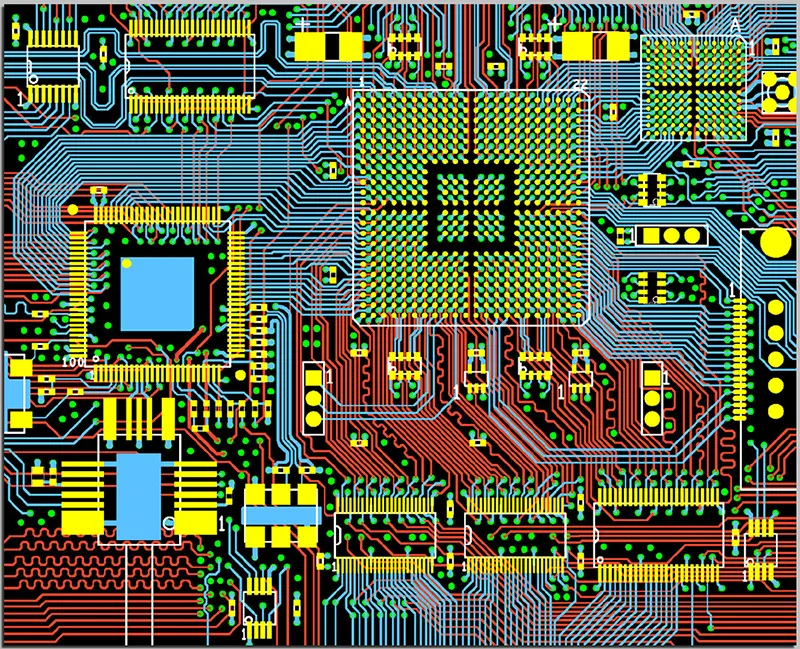
Abstract: Signal layer planning in 4-layer PCBs critICally impacts signal integrity (SI), EMC, and crosstalk control. The core principle is "orthogonal routing between adjacent signal layers" (e.g., top layer horizontal, bottom layer vertical), combined with solid reference planes and the 20H rule for impedance control and crosstalk suppression. This article details the planning strategy and technical basis.
1. Standard Stackup & Layer Assignment
| Layer | Function | Thickness (mm) | Key Properties |
|---|---|---|---|
| L1 | Signal (Horizontal) | 0.035 | 1oz Cu; priority for critical signals |
| L2 | Solid GND Plane | 0.15 | Low-impedance return path |
| L3 | Solid Power Plane | 0.15 | Split spacing ≥0.5mm |
| L4 | Signal (Vertical) | 0.035 | 1oz Cu; low-speed signals |
Design Redlines:
L1 and L4 must be orthogonal (90° cross); minimize parallel routing.
L2/L3 planes must remain solid (no splits under high-speed signals).
2. Signal Routing Principles
-
Orthogonal Routing Rule:
-
If L1 routes at 0° (horizontal), L4 must be 90° (vertical);
-
Parallel segments ≤15mm (prevents ↑30% crosstalk); spacing ≥3W (W=trace width).
-
-
Layer Transition Handling:
-
Add GND vias (≥0.2mm hole) within 5mm of transition points;
-
Never route L1→L4 directly; transition through L2/L3 reference planes.
-
3. Critical Signal Strategies
-
High-Speed Signals (>50MHz):
-
Prioritize L1 (top layer); avoid crossing splits (if unavoidable, spacing ≥3mm);
-
Guard traces: Add GND shields on both sides (spacing 2W); GND vias every 20mm.
-
-
Clock Signals:
-
Route on L1 referenced to L2 GND; length matching tolerance ±0.1mm;
-
No >10mm parallel runs with high-speed signals.
-
-
Differential Pairs:
-
Intra-pair spacing =2W; inter-pair spacing ≥5W;
-
Synchronous layer transitions; via spacing ≤0.3mm (minimizes phase skew).
-
4. Power/Ground Plane Management
-
Plane Splitting:
-
Spacing between voltage domains ≥0.5mm (e.g., 3.3V/5.0V);
-
Avoid parallel runs with signals (angle ≥45°).
-
-
20H Rule:
-
Power plane (L3) recessed by 20×dielectric thickness (20×0.15mm=3mm) from GND (L2) to reduce edge radiation.
-
-
Decoupling Capacitors:
-
Place within ≤1.5mm of IC power pins; GND terminals directly connected to L2 plane (via ≤0.5mm away).
-
5. EMC & SI Optimization
-
Crosstalk Control:
-
Orthogonal routing reduces crosstalk by 10–15dB vs. parallel routing;
-
Spacing ≥5mm between sensitive signals (reset, analog) and noise sources (switchers).
-
-
Impedance Continuity:
-
Top/bottom (L1/L4) microstrip impedance:
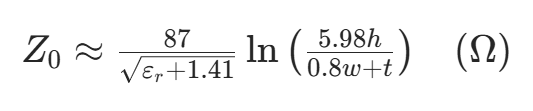
(h: dielectric thickness, w: width, t: Cu thickness, ε_r: Dk)
-
Internal striplines require symmetric stackup calculation.
-
-
Termination:
-
Add source-end 33Ω series resistor for >100MHz signals to suppress ringing.
-
6. Verification & Simulation
-
Stackup Impedance Simulation:
-
Use Polar SI9000 for line width (FR-4, ε_r=4.2):
-
L1 50Ω microstrip: w=0.26mm (h=0.15mm)
-
Internal 100Ω diff-pair: w=0.12mm, s=0.1mm
-
-
-
Crosstalk Simulation:
-
Near-end crosstalk NEXT≤-40dB for 15mm parallels (HyperLynx verification).
-
-
Return Path Check:
-
No gaps >0.1mm in reference plane under layer-transition signals.
-
Conclusion
4-layer PCB signal routing demands strict adherence to "orthogonal routing + solid reference planes":
-
L1 and L4 must cross orthogonally; parallel segments ≤15mm;
-
L2/L3 must be solid; split spacing ≥0.5mm with 20H rule;
-
Critical Measures:
-
Route high-speed signals on outer layers,
-
Add GND vias within 5mm of layer transitions,
-
Avoid 0° angles between power splits and signals.
-