 PCB
PCB FPC
FPC Rigid-Flex
 FR-4
FR-4 HDI PCB
 Rogers High-Frequency Board
 PTFE Teflon High-Frequency Board
 Aluminum
 Copper Core
 PCB Assembly
 LED light PCBA
 Memory PCBA
 Power Supply PCBA
 New Energey PCBA
 Communication PCBA
 Industrial Control PCBA
 Medical Equipment PCBA
 Testing Service
 PCBA Testing Service
 Certification Application
 RoHS Certification Application
 REACH Certification Application
 CE Certification Application
 FCC Certification Application
 CQC Certification Application
 UL Certification Application
 Transformers, Inductors
 High Frequency Transformers
 Low Frequency Transformers
 High Power Transformers
 Conversion Transformers
 Sealed Transformers
 Ring Transformers
 Inductors
 Wires,Cables Customized
 Network Cables
 Power Cords
 Antenna Cables
 Coaxial Cables
 Net Position Indicator
 Solar AIS net position indicator
 Capacitors
 Connectors
 Diodes
 Embedded Processors & Controllers
 Digital Signal Processors (DSP/DSC)
 Microcontrollers (MCU/MPU/SOC)
 Programmable Logic Device(CPLD/FPGA)
 Communication Modules/IoT
 Resistors
 Through Hole Resistors
 Resistor Networks, Arrays
 Potentiometers,Variable Resistors
 Aluminum Case,Porcelain Tube Resistance
 Current Sense Resistors,Shunt Resistors
 Switches
 Transistors
 Power Modules
 Isolated Power Modules
 AC-DC Power Modules
 DC-AC Module(Inverter)
 RF and Wireless
Manufacturing High-Precision Embedded Resistors via Aerosol Jet Printing Technology
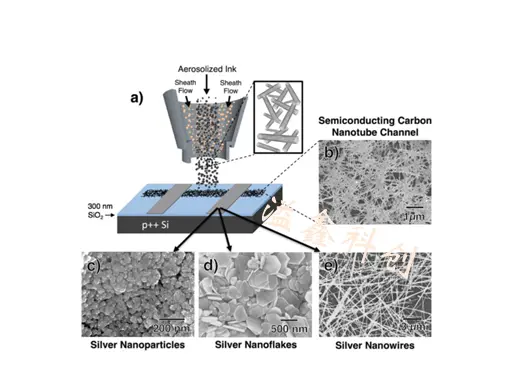
1. Principles and Advantages of Aerosol Jet Printing
Aerosol Jet Printing (AJP) deposits functional inks as mICron-scale aerosols (1–5 μm) using sheath gas focusing, enabling:
-
High resolution: 10 μm linewidth with ±2 μm placement accuracy;
-
Material versatility: Compatible with metals (Ag, Cu), carbon-based (graphene, CNT), and Resistor pastes (RuO₂, NiCr);
-
Non-contact deposition: Suitable for flexible (PI, PET) and rigid (FR-4, ceramics) substrates.
2. Fabrication Process Flow
(1) Resistor Material Design and Ink Formulation
-
Materials:
-
Carbon-based: Graphene/CNT composites (10–1000 Ω/□, TCR±100 ppm/°C);
-
Metal-ceramic: RuO₂/NiCr inks (50–500 Ω/□, TCR±50 ppm/°C);
-
Polymer: PEDOT:PSS (1–10 kΩ/□, TCR±200 ppm/°C).
-
-
Ink optimization:
-
Viscosity control (10–100 cP) for stable atomization;
-
Dispersants (e.g., PVP) prevent nanoparticle agglomeration.
-
(2) Aerosol Generation and Deposition Control
-
Atomization:
-
Ultrasonic (1–3 MHz) or pneumatic (10–50 psi carrier gas) atomization;
-
Ink flow rate (0.1–1 mL/min) adjusts deposition speed.
-
-
Focused deposition:
-
Sheath-to-aerosol flow ratio (3:1 to 10:1) minimizes coffee-ring effect;
-
Substrate heating (50–80°C) accelerates solvent evaporation.
-
(3) Patterning and Path Planning
-
CAD-to-path conversion: Optimize scan speed (10–50 mm/s) and overlap (20–30%);
-
Dynamic parameter adjustment: Nozzle height (100–500 μm) and gas flow tuned for linewidth consistency.
(4) Post-Processing and Tuning
-
Annealing:
-
200–300°C in N₂ removes organics, reduces resistivity (e.g., Ag <5 μΩ·cm);
-
-
Laser trimming:
-
Femtosecond laser (1030 nm, 300 fs) enables ±0.1% resistance adjustment;
-
Real-time four-wire monitoring for closed-loop control.
-
3. Key Techniques for Precision Control
(1) Resistance Uniformity
-
In-line monitoring: Optical microscopy + resistance testing for real-time feedback;
-
Multi-nozzle coordination: Machine learning compensates nozzle variations.
(2) Interface Adhesion Enhancement
-
Substrate pretreatment:
-
Plasma activation (O₂/N₂) reduces contact angle to <10°;
-
SAM layers improve ink wettability.
-
-
Multi-layer stacking: Alternating conductive/passivation layers (e.g., SiO₂) for humidity resistance.
(3) Environmental Stability
-
Encapsulation: UV-cured epoxy (5–10 μm) for moisture/oxygen barrier (MIL-STD-883 compliant);
-
Aging tests: <1% drift after 1000 hours at 85°C/85% RH.
4. Challenges and Solutions
-
Challenge 1: Nanoparticle non-uniformity:
-
Solution: Ultrasonic dispersion + electrostatic focusing (±500 V);
-
-
Challenge 2: Limited high-resistance resolution:
-
Solution: Submicron nozzles (20 μm) + low-viscosity inks (<20 cP);
-
-
Challenge 3: Alignment errors on flexible substrates:
-
Solution: Vision systems (±1 μm) + real-time deformation compensation.
-
5. Applications and Performance Metrics
-
RF matching resistors: 50 Ω±1% resistors with <-20 dB return loss up to 40 GHz;
-
Flexible sensor bridges: 1 kΩ±0.5% resistors stable under <5 mm bending;
-
Cost efficiency: >90% material utilization, 30% cost reduction vs. screen printing.