 PCB
PCB FPC
FPC Rigid-Flex
 FR-4
FR-4 HDI PCB
 Rogers High-Frequency Board
 PTFE Teflon High-Frequency Board
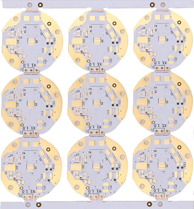
 Aluminum
 Copper Core
 PCB Assembly
 LED light PCBA
 Memory PCBA
 Power Supply PCBA
 New Energey PCBA
 Communication PCBA
 Industrial Control PCBA
 Medical Equipment PCBA
 Testing Service
 PCBA Testing Service
 Certification Application
 RoHS Certification Application
 REACH Certification Application
 CE Certification Application
 FCC Certification Application
 CQC Certification Application
 UL Certification Application
 Transformers, Inductors
 High Frequency Transformers
 Low Frequency Transformers
 High Power Transformers
 Conversion Transformers
 Sealed Transformers
 Ring Transformers
 Inductors
 Wires,Cables Customized
 Network Cables
 Power Cords
 Antenna Cables
 Coaxial Cables
 Net Position Indicator
 Solar AIS net position indicator
 Capacitors
 Connectors
 Diodes
 Embedded Processors & Controllers
 Digital Signal Processors (DSP/DSC)
 Microcontrollers (MCU/MPU/SOC)
 Programmable Logic Device(CPLD/FPGA)
 Communication Modules/IoT
 Resistors
 Through Hole Resistors
 Resistor Networks, Arrays
 Potentiometers,Variable Resistors
 Aluminum Case,Porcelain Tube Resistance
 Current Sense Resistors,Shunt Resistors
 Switches
 Transistors
 Power Modules
 Isolated Power Modules
 AC-DC Power Modules
 DC-AC Module(Inverter)
 RF and Wireless
Allowable Thickness Tolerance of Insulation Layers in Metal Core PCB Lamination to Ensure Drilling Accuracy
2025-11-12
Metal core printed Circuit Boards (MCPCBs) are widely used in high-power electronic applications due to their excellent thermal conductivity, with aluminum and copper cores being the most common. The lamination process of MCPCBs involves bonding the metal core, insulation layer (typically epoxy resin, PI, or ceramic-filled composites), and copper foil into an integrated structure. Among these layers, the insulation layer’s thickness deviation during lamination directly affects the accuracy of subsequent drilling—excessive deviation can lead to hole size errors, misalignment, or even insulation layer damage. This article details the allowable thickness tolerance range of the insulation layer, influencing factors, and control measures based on industry standards (e.g., IPC-2225) and manufacturing practice.
1. The Link Between Insulation Layer Thickness Deviation and Drilling Accuracy
To understand the required tolerance, it is first necessary to clarify how insulation layer thickness variation impacts drilling:
- Drilling mechanism in MCPCBs: Drilling in MCPCBs targets precise penetration through the copper foil, insulation layer, and metal core (or stopping at the metal core suRFace for blind holes). The drill bit’s feed rate and cutting parameters are calibrated based on the designed insulation layer thickness.
- Deviation-induced errors: If the insulation layer is thicker than designed, the drill bit may not reach the target depth (causing shallow holes) or require excessive force, leading to bit wear and enlarged hole diameters. If thinner than designed, the drill bit over-penetrates, damaging the metal core or causing inconsistent hole wall quality.
- Key accuracy requirements: For most MCPCB applications, the acceptable drilling aperture deviation is ±0.05mm (for holes ≤1.0mm diameter) or ±5% of the nominal aperture (for holes >1.0mm). The insulation layer’s thickness tolerance must be controlled to ensure this aperture precision.
2. Allowable Thickness Tolerance Range of Insulation Layers
The allowable thickness deviation of the insulation layer depends on its designed thickness, drilling type (through-hole vs. blind hole), and aperture size. Industry-recognized standard ranges are as follows:
2.1 Standard Insulation Layer Thickness (0.1–0.5mm)
This is the most common thickness range for MCPCBs (used in LEDs, power modules, and automotive electronics):
- Through-hole drilling (aperture 0.3–1.0mm): The allowable thickness tolerance is ±0.03mm. For example, a designed 0.2mm insulation layer must be controlled between 0.17mm and 0.23mm. This ensures the drill bit’s cutting path aligns with calibrated parameters, limiting aperture deviation to ±0.05mm.
- Blind hole drilling (aperture 0.2–0.8mm, stopping at metal core): The tolerance is stricter at ±0.02mm. A 0.3mm designed insulation layer must be 0.28–0.32mm, as blind holes require precise depth control to avoid incomplete penetration or metal core damage.
2.2 Thin Insulation Layers (<0.1mm)
Thin insulation layers (0.05–0.1mm) are used in high-power-density MCPCBs for reduced thermal resistance:
- Allowable tolerance: ±0.015mm. For a 0.08mm insulation layer, the acceptable range is 0.065–0.095mm.
- Rationale: Thin layers have smaller thermal mass and are more prone to lamination unevenness. A tighter tolerance prevents the insulation layer from being too thin (risk of breakdown during drilling) or too thick (causing blind hole depth errors).
2.3 Thick Insulation Layers (>0.5mm)
Thick insulation layers (0.5–1.0mm) are used in high-voltage MCPCBs (e.g., industrial power supplies):
- Allowable tolerance: ±0.05mm. For a 0.8mm insulation layer, the range is 0.75–0.85mm.
- Rationale: Thicker layers have higher structural stability, and drilling errors are less sensitive to thickness variation. However, exceeding ±0.05mm can still cause aperture deviation exceeding ±0.08mm (unacceptable for most high-voltage applications).
2.4 Special Case: Microvias (Aperture ≤0.2mm)
For microvia drilling (common in miniaturized MCPCBs), the insulation layer thickness tolerance must be ±0.01mm regardless of designed thickness. This ultra-strict control ensures the microvia’s aspect ratio (depth-to-diameter) remains within 1:1, avoiding drill bit deflection and hole wall roughness.
3. Factors Influencing Tolerance Requirements
The allowable thickness tolerance is not fixed; it adjusts based on three key factors:
3.1 Drilling Equipment and Tooling
- High-precision CNC drills (with ±0.005mm positioning accuracy) can compensate for minor insulation layer deviations (±0.005mm), allowing a slightly wider tolerance.
- Standard drills require stricter insulation layer control, as they have lower feed rate adjustability.
- Drill bit type: Carbide-tipped drill bits (harder and more wear-resistant) are less sensitive to thickness variation than HSS drill bits, enabling a 10–15% looser tolerance.
3.2 Insulation Layer Material Properties
- Rigid materials (e.g., ceramic-filled epoxy) have better lamination uniformity, so tolerance can be relaxed by 5–10% compared to flexible materials (e.g., PI).
- Thermal expansion coefficient (TCE): Materials with TCE matching the metal core (e.g., aluminum-core compatible epoxy) experience less thickness variation during lamination, allowing wider tolerance.
3.3 Lamination Process Parameters
- Pressure and temperature uniformity: Lamination under controlled pressure (20–30kg/cm²) and temperature (140–180°C) with even heat distribution reduces insulation layer thickness deviation by 30–40%.
- Lamination speed: Slow, gradual lamination (1–2°C/min heating rate) minimizes resin flow unevenness, enabling tighter tolerance control.
4. Practical Control Measures to Maintain Tolerance
To ensure the insulation layer’s thickness deviation stays within the allowable range, implement the following manufacturing practices:
4.1 Pre-Lamination Material Inspection
- Verify the insulation layer’s raw material thickness tolerance (supplier should provide ±0.02mm for standard materials) before lamination.
- Check for material defects (e.g., bubbles, uneven thickness) using a laser thickness gauge (accuracy ±0.001mm).
4.2 Lamination Process Optimization
- Use a precision lamination press with programmable pressure and temperature curves to ensure uniform resin flow.
- Place pressure distribution mats between the lamination plates to compensate for metal core flatness deviations (≤0.02mm).
- Control the lamination time (60–90 minutes for standard epoxy) to avoid under-curing (which causes thickness instability) or over-curing (which increases brittleness).
4.3 Post-Lamination Thickness Verification
- Measure the insulation layer thickness at 5–8 evenly distributed points across the MCPCB using a micrometer (accuracy ±0.001mm).
- Reject boards where any measurement exceeds the allowable tolerance, as localized deviations can still cause drilling errors.
4.4 Drilling Parameter Adjustment
- For boards with minor insulation layer deviations (within 80% of allowable tolerance), adjust the drill bit feed rate (±10%) or spindle speed (±5%) to compensate.
- Use automated drilling systems with real-time depth sensing to dynamically adjust parameters based on actual insulation layer thickness.
5. Consequences of Exceeding Tolerance
Failing to control insulation layer thickness deviation leads to critical manufacturing defects:
- Aperture deviation >±0.08mm: Causes poor solder joint formation, component misalignment, and reduced current-carrying capacity.
- Hole wall damage: Excessive thickness leads to drill bit overheating, causing insulation layer delamination or resin burning.
- Reduced reliability: Uneven insulation thickness increases voltage breakdown risk (for high-voltage MCPCBs) and thermal resistance variation (for high-power applications).
To ensure subsequent drilling aperture accuracy in metal core PCB lamination, the insulation layer’s thickness deviation must be strictly controlled within industry-specific ranges: ±0.01–0.05mm depending on designed thickness, drilling type, and aperture size. For standard 0.1–0.5mm insulation layers, ±0.03mm (through-holes) and ±0.02mm (blind holes) are recommended; thin layers (<0.1mm) require ±0.015mm, thick layers (>0.5mm) allow ±0.05mm, and microvias demand ±0.01mm. Key influencing factors include drilling equipment, insulation material properties, and lamination process uniformity. By implementing strict material inspection, optimized lamination parameters, and post-lamination verification, manufacturers can maintain tolerance control and ensure drilling accuracy—critical for MCPCB performance and reliability.