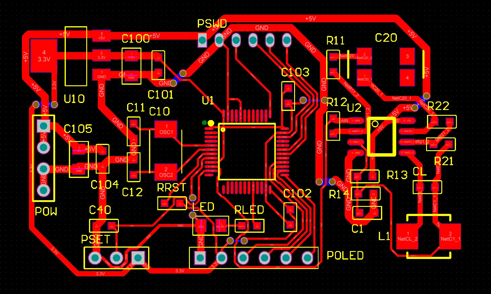
 PCB
PCB FPC
FPC Rigid-Flex
 FR-4
FR-4 HDI PCB
 Rogers High-Frequency Board
 PTFE Teflon High-Frequency Board
 Aluminum
 Copper Core
 PCB Assembly
 LED light PCBA
 Memory PCBA
 Power Supply PCBA
 New Energey PCBA
 Communication PCBA
 Industrial Control PCBA
 Medical Equipment PCBA
 Testing Service
 PCBA Testing Service
 Certification Application
 RoHS Certification Application
 REACH Certification Application
 CE Certification Application
 FCC Certification Application
 CQC Certification Application
 UL Certification Application
 Transformers, Inductors
 High Frequency Transformers
 Low Frequency Transformers
 High Power Transformers
 Conversion Transformers
 Sealed Transformers
 Ring Transformers
 Inductors
 Wires,Cables Customized
 Network Cables
 Power Cords
 Antenna Cables
 Coaxial Cables
 Net Position Indicator
 Solar AIS net position indicator
 Capacitors
 Connectors
 Diodes
 Embedded Processors & Controllers
 Digital Signal Processors (DSP/DSC)
 Microcontrollers (MCU/MPU/SOC)
 Programmable Logic Device(CPLD/FPGA)
 Communication Modules/IoT
 Resistors
 Through Hole Resistors
 Resistor Networks, Arrays
 Potentiometers,Variable Resistors
 Aluminum Case,Porcelain Tube Resistance
 Current Sense Resistors,Shunt Resistors
 Switches
 Transistors
 Power Modules
 Isolated Power Modules
 AC-DC Power Modules
 DC-AC Module(Inverter)
 RF and Wireless
Mitigating Inter-Symbol Interference (ISI) in Ultra-High-Speed PCB Designs (112Gbps+)
I. ISI Mechanism & QuantifICation
-
Loss-Dominated Formula
-
: Loss per unit length (dB/inch)
-
: Trace length
-
: Baud rate (56GBaud for PAM4 @112Gbps)
-
-
Key Impact Factors
Factor ISI Contribution Control Target Dielectric Loss (Df) 45% Df≤0.001 @10GHz Skin Effect Roughness 30% Ra≤0.3μm (HVLP Cu) Impedance Discontinuity 15% ΔZ≤±3Ω Reflection Noise 10% Return Loss<-20dB
II. Material & Stackup Optimization
-
Substrate Selection
Material Df@10GHz Data Rate Cost Factor Megtron 7 0.001 ≤112Gbps 1.8x Rogers Kappa 438 0.002 56-112Gbps 1.3x Standard FR4 0.025 ≤28Gbps 1.0x -
Stackup Example (12-Layer)
L1: Signal (short traces) ↓ Prepreg: 2mil Ultra-Loss (Df=0.001) L2: Solid Ground Plane ← Critical! ↓ Core: 3mil Megtron 7 L3: Signal (112G diff pairs) ↓ Prepreg: 2.5mil L4: Power Plane (split zone with cap arrays)Rules:
-
High-speed layer-to-ground distance ≤4mil
-
Orthogonal routing on adjacent layers (angle≥75°)
-
III. Critical Routing Techniques
-
Impedance & Loss Control
-
Diff Pair Specs:
Width/Spacing(mil) Impedance(Ω) Loss(dB/inch@28GHz) 5/5 85±2 0.65 4/6 100±1 0.58 -
Back-Drilling:
-
-
Length & Phase Matching
-
Intra-pair skew: ≤0.05mm (0.3ps @112Gbps)
-
Serpentine Rules:
-
Spacing ≥3×width
-
Bend radius ≥5×width
-
-
-
Via Optimization
Standard Via → UHS Via Hole: 8mil → 5mil Pad: 18mil → 12mil Add: Back-drill +2mil, GND via array (pitch=25mil)Effect: Return loss improved by 15dB@56GHz
IV. Signal Integrity Enhancement
-
Transmitter Equalization (FFE)
-
Optimized 3-tap FFE:
-
-
Receiver Equalization (CTLE+DFE)
Type Gain Compensation Application CTLE 3-8dB @ Nyquist Mid-range backplane DFE Post-cursor removal >20" long traces -
Pre/De-emphasis
-
De-emphasis formula:
-
V. Verification & SIMulation Flow
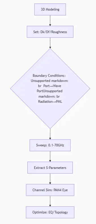
Targets:
-
Total loss: < -25dB @56GHz
-
Eye height: >25mV @BER=1E-12
-
Jitter: <0.15UI
VI. Test Data (112G PAM4 Optical Module)
| Control Method | Eye Height(mV) | Jitter(UI) | BER |
|---|---|---|---|
| Conventional | 18.2 | 0.28 | 3.2E-10 |
| Full Optimization | 36.5 | 0.12 | <1E-15 |
Validation:
-
VNA: Keysight N5225B (110GHz)
-
BERT: Anritsu MP1900A (PAM4 112Gbps)
-
TDR: Tektronix 70GHz sampling scope