 PCB
PCB FPC
FPC Rigid-Flex
 FR-4
FR-4 HDI PCB
 Rogers High-Frequency Board
 PTFE Teflon High-Frequency Board
 Aluminum
 Copper Core
 PCB Assembly
 LED light PCBA
 Memory PCBA
 Power Supply PCBA
 New Energey PCBA
 Communication PCBA
 Industrial Control PCBA
 Medical Equipment PCBA
 Testing Service
 PCBA Testing Service
 Certification Application
 RoHS Certification Application
 REACH Certification Application
 CE Certification Application
 FCC Certification Application
 CQC Certification Application
 UL Certification Application
 Transformers, Inductors
 High Frequency Transformers
 Low Frequency Transformers
 High Power Transformers
 Conversion Transformers
 Sealed Transformers
 Ring Transformers
 Inductors
 Wires,Cables Customized
 Network Cables
 Power Cords
 Antenna Cables
 Coaxial Cables
 Net Position Indicator
 Solar AIS net position indicator
 Capacitors
 Connectors
 Diodes
 Embedded Processors & Controllers
 Digital Signal Processors (DSP/DSC)
 Microcontrollers (MCU/MPU/SOC)
 Programmable Logic Device(CPLD/FPGA)
 Communication Modules/IoT
 Resistors
 Through Hole Resistors
 Resistor Networks, Arrays
 Potentiometers,Variable Resistors
 Aluminum Case,Porcelain Tube Resistance
 Current Sense Resistors,Shunt Resistors
 Switches
 Transistors
 Power Modules
 Isolated Power Modules
 AC-DC Power Modules
 DC-AC Module(Inverter)
 RF and Wireless
Key Technologies and Practices for Reducing BGA Solder Joint Void Rate via Nitrogen Reflow Soldering
2025-09-06
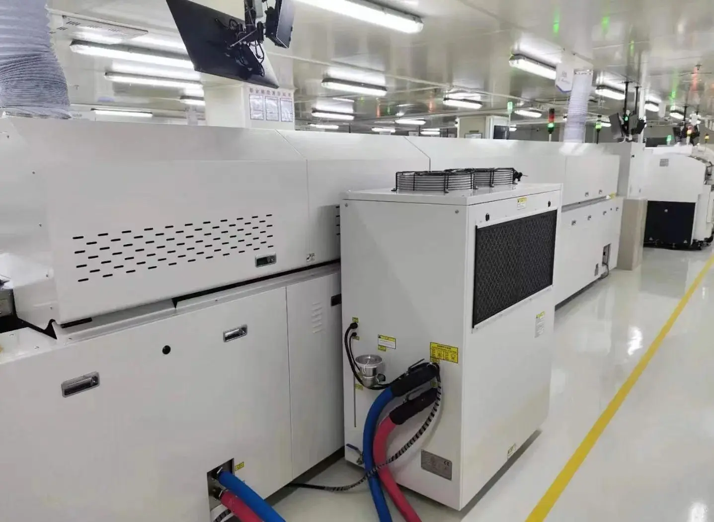
1. Introduction: Hazards of BGA Solder Joint Voids and Advantages of Nitrogen Reflow Soldering
Ball Grid Array (BGA) packaging is widely used in consumer electronICs, communication equipment, and automotive electronics due to its high pin density and excellent heat dissipation. However, BGA solder joint voids are a common quality defect during the soldering process, caused by factors such as poor discharge of solder paste volatiles and oxidation reactions. Voids not only reduce the mechanical strength and electrical conductivity of solder joints but may also lead to intermittent circuit failures or complete malfunction, directly affecting product reliability and service life.
Nitrogen reflow soldering creates an inert gas atmosphere in the soldering area, effectively suppressing oxidation reactions and improving solder paste wettability, providing a key solution to reduce BGA solder joint void rates. Compared with traditional air reflow soldering, the nitrogen environment can significantly reduce the oxidation degree of solder pads and solder balls, accelerate the discharge of flux volatiles in the solder paste, and fundamentally reduce the occurrence of voids.
2. Core Principles of Nitrogen Reflow Soldering for Reducing BGA Void Rate
2.1 Suppressing Oxidation Reactions
During high-temperature soldering, pad materials (usually copper), BGA solder balls (mostly tin-lead or lead-free alloys), and metal components in the solder paste are prone to oxidation with oxygen in the air, forming metal oxides (such as CuO and SnO₂). These oxides hinder the wetting and spreading of solder, leading to discontinuous inteRFaces between solder and pads, which then trap air to form voids. As an inert gas, nitrogen can effectively displace air in the soldering area, controlling the oxygen content below 100ppm (as low as 10ppm in precision soldering scenarios), suppressing oxidation reactions from the source, and ensuring good metallurgical bonding between solder and pads.
2.2 Improving Solder Paste Wettability and Volatile Discharge
The flux in the solder paste undergoes three stages during reflow: "activation-volatilization-curing". In an air environment, the oxide layer reduces the wettability of the solder paste, making it difficult for flux volatiles (such as solvents and organic acids) to discharge quickly, which are trapped inside the solder to form voids. In a nitrogen environment, the clean interface without an oxide layer significantly improves the wettability of the solder paste, allowing the solder to spread quickly. At the same time, the flow of nitrogen (usually achieved through air knives or cavity airflow circulation) accelerates the discharge of volatiles, reducing the residual amount of volatiles before solder solidification, thereby lowering the probability of void formation.
3. Key Process Control Measures for Reducing BGA Solder Joint Void Rate
3.1 Optimization of Nitrogen Environment Parameters
- Oxygen Content Control: Oxygen content is a core parameter affecting the effect of nitrogen reflow soldering. For lead-free BGA soldering (melting point usually 217-221℃), the oxygen content is recommended to be controlled at 50-100ppm; for high-density, fine-pitch BGA (such as CSP, PoP packaging), it needs to be further reduced to 10-30ppm to ensure the soldering quality of micro solder joints. In actual production, real-time monitoring can be carried out through an online oxygen content monitor, and the nitrogen flow rate (usually 5-20L/min) can be adjusted to maintain a stable inert atmosphere.
- Nitrogen Flow Rate and Cavity Pressure: The nitrogen flow rate should match the volume of the reflow oven cavity. Too small a flow rate may lead to air residue, while too large a flow rate will cause nitrogen waste and may affect temperature uniformity. At the same time, some high-end reflow ovens support micro-positive pressure control (pressure range 50-200Pa), which further prevents external air infiltration by maintaining the cavity slightly above atmospheric pressure, improving the stability of the nitrogen atmosphere.
3.2 Optimization of Reflow Temperature Profile
The reflow temperature profile directly affects the melting of solder paste, discharge of volatiles, and solidification of solder joints. It needs to be accurately adjusted according to the BGA package type and solder paste characteristics, which is mainly divided into four stages:
- Preheat Stage: The temperature rises from room temperature to 120-150℃, with a heating rate controlled at 1-3℃/s. This stage requires slow heating to gradually volatilize the solvent in the solder paste, avoiding rapid volatilization to form bubbles; at the same time, activate the flux to remove the slight oxide layer on the surface of the pad and solder ball.
- Soak Stage: The temperature is maintained at 150-180℃ for 60-120s. The purpose is to make the overall temperature of the PCB and BGA uniform, preventing inconsistent solder melting caused by temperature difference; at the same time, further discharge the flux volatiles to reduce the void risk in the subsequent high-temperature stage.
- Reflow Stage: The temperature quickly rises to the peak temperature (usually 240-260℃ for lead-free solder, 20-40℃ higher than the melting point), and the peak time is maintained for 30-60s. At this stage, the solder is completely melted, and it is necessary to ensure that the solder is fully wetted and spread. At the same time, the residual volatiles are completely discharged with the help of nitrogen flow. The heating rate should be controlled at 2-5℃/s to avoid solder splashing or bubble trapping caused by sudden temperature rise.
- Cooling Stage: The temperature quickly drops from the peak to room temperature, with a cooling rate controlled at 3-6℃/s. Rapid cooling can make the solder joints form a fine grain structure, improving mechanical strength; at the same time, avoiding the solder joints staying in the high-temperature area for too long, leading to oxidation or excessive growth of intermetallic compounds (IMC).
3.3 Pretreatment of PCB and BGA Components
- PCB Pad Cleaning and Protection: PCBs are prone to absorb moisture and oxidize during storage. Before soldering, they need to be dried (usually 85℃/12h or 125℃/4h) to remove moisture; at the same time, check whether the pad surface has oxidation discoloration (such as blackening, yellowing). If the oxidation is severe, plasma cleaning or chemical cleaning (such as weak acid cleaning agent) should be used to remove the oxide layer to ensure the pad is clean.
- BGA Component Baking: BGA components (especially plastic packages) absorb moisture from the air during storage. Moisture expands when heated during high-temperature soldering, which may cause package cracking ("popcorn effect") and increase the solder joint void rate. Baking should be carried out according to the component's Moisture Sensitivity Level (MSL). For example, MSL 3 components that are not used within 24 hours after opening should be baked at 125℃ for 24 hours.
3.4 Solder Paste Selection and Printing Process Control
The composition and performance of solder paste directly affect the void rate. Lead-free solder paste with low volatiles and high activity (such as Sn-Ag-Cu series) should be selected, and its flux should have good oxidation resistance and volatile discharge characteristics. In terms of printing process, the following parameters need to be controlled:
- Stencil Design: The stencil openings corresponding to BGA pads should adopt "solder ball prevention design", such as reducing the opening size (usually 90%-95% of the pad size), increasing the opening thickness (0.12-0.15mm), or using a stepped stencil to ensure uniform and not excessive solder paste printing. Excessive solder paste easily leads to more volatiles, while insufficient solder paste may cause cold joints.
- Printing Parameters: The printing speed is controlled at 20-40mm/s, the SCRaper pressure at 0.1-0.3MPa, and the demolding speed at 5-10mm/s. After printing, check whether the solder paste pattern is complete, whether there is missing tin, bridging or bubbles. If there are defects, clean them in time and reprint.
4. Quality Inspection and Continuous Improvement
After soldering, professional equipment is needed to detect the void rate of BGA solder joints. Common methods include:
- X-ray Detection (X-RAY): X-rays penetrate the BGA package to clearly show the void distribution and size inside the solder joints, which is the mainstream method for detecting BGA solder joint voids. Usually, the void area of a single solder joint should not exceed 25% of the total area of the solder joint, and the void rate of the entire board should be below 5%.
- Cross-Section Analysis: For severe voids found in X-ray detection, cross-section analysis can be used to determine the causes of voids (such as oxidation, volatile residue, insufficient solder paste, etc.), providing a basis for process optimization.
In addition, statistical process control (SPC) of process parameters should be established to regularly monitor key parameters such as oxygen content, temperature profile, and solder paste printing quality. Use quality tools such as fishbone diagrams and Pareto charts to analyze the causes of excessive void rates, continuously optimize the process, and achieve stable control of the void rate.
5. Common Error and Omission Checks and Avoidance
Common Error 1: Neglecting nitrogen flow rate and cavity tightness. If the reflow oven cavity has leaks, it is difficult to reduce the oxygen content even if the nitrogen flow rate is increased. Regularly check whether the cavity sealing strip is aging and whether the door control is tight to ensure the stability of the nitrogen atmosphere.
Common Error 2: Mismatch between temperature profile setting and solder paste characteristics. Different brands and models of solder paste correspond to different reflow temperature windows. Blindly applying a general curve may lead to incomplete flux volatilization or insufficient solder melting. Adjustments should be made according to the recommended curve provided by the solder paste supplier.
Common Error 3: Incomplete pretreatment of PCB and BGA. Moisture and oxide layers are important incentives for voids. Strictly follow the processing specifications for moisture-sensitive components for baking and cleaning to avoid increased void rates due to omissions in the pretreatment link.
6. Conclusion
Nitrogen reflow soldering is an effective technical means to reduce the BGA solder joint void rate, but its effect depends on the coordinated optimization of nitrogen environment parameters, reflow temperature profile, component pretreatment, and solder paste process. By accurately controlling the key parameters of each link, combined with strict quality inspection and continuous improvement mechanisms, the BGA solder joint void rate can be controlled at a low level, significantly improving the soldering quality and reliability of electronic products. In the field of high-density and high-reliability electronic manufacturing, the rational application of nitrogen reflow soldering technology will become an important guarantee for enterprises to improve product competitiveness.