 PCB
PCB FPC
FPC Rigid-Flex
 FR-4
FR-4 HDI PCB
 Rogers High-Frequency Board
 PTFE Teflon High-Frequency Board
 Aluminum
 Copper Core
 PCB Assembly
 LED light PCBA
 Memory PCBA
 Power Supply PCBA
 New Energey PCBA
 Communication PCBA
 Industrial Control PCBA
 Medical Equipment PCBA
 Testing Service
 PCBA Testing Service
 Certification Application
 RoHS Certification Application
 REACH Certification Application
 CE Certification Application
 FCC Certification Application
 CQC Certification Application
 UL Certification Application
 Transformers, Inductors
 High Frequency Transformers
 Low Frequency Transformers
 High Power Transformers
 Conversion Transformers
 Sealed Transformers
 Ring Transformers
 Inductors
 Wires,Cables Customized
 Network Cables
 Power Cords
 Antenna Cables
 Coaxial Cables
 Net Position Indicator
 Solar AIS net position indicator
 Capacitors
 Connectors
 Diodes
 Embedded Processors & Controllers
 Digital Signal Processors (DSP/DSC)
 Microcontrollers (MCU/MPU/SOC)
 Programmable Logic Device(CPLD/FPGA)
 Communication Modules/IoT
 Resistors
 Through Hole Resistors
 Resistor Networks, Arrays
 Potentiometers,Variable Resistors
 Aluminum Case,Porcelain Tube Resistance
 Current Sense Resistors,Shunt Resistors
 Switches
 Transistors
 Power Modules
 Isolated Power Modules
 AC-DC Power Modules
 DC-AC Module(Inverter)
 RF and Wireless
Optimizing Impedance Control of High-Speed PCBs Through Stackup Design
2025-09-18
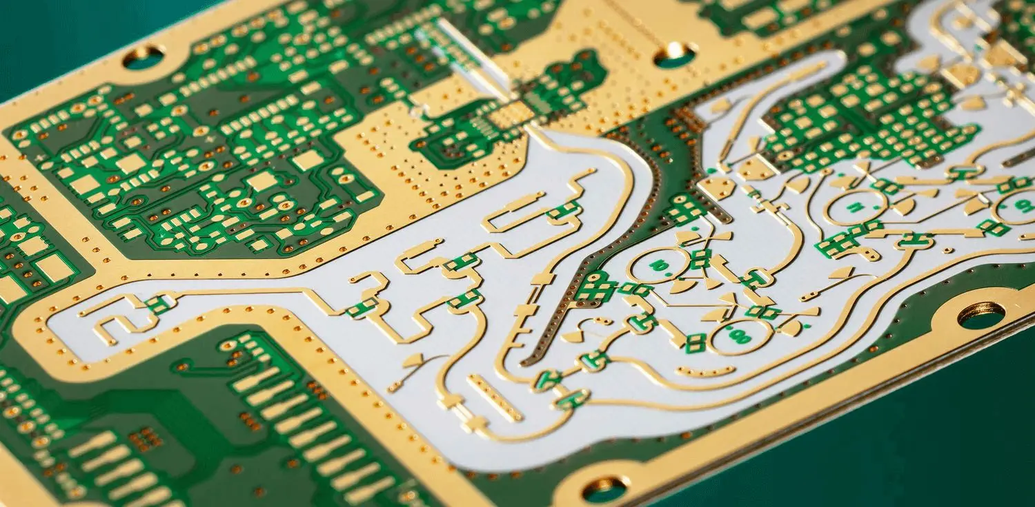
The Relationship Between High-Speed PCB Impedance Control and Stackup Design
In high-speed PCBs (signal rate ≥5Gbps), impedance matching is a core prerequisite for ensuring signal integrity (SI). When the impedance of the signal transmission line does not match the source and load impedances, signal reflection occurs, leading to problems such as return loss (RL) degradation, eye diagram distortion, and timing offset. Industry standards require that the impedance tolerance of high-speed signal transmission lines be controlled within ±5% (e.g., the actual impedance of a 50Ω transmission line should be between 47.5-52.5Ω).
Stackup design is the foundation of impedance control — the characteristIC impedance of a transmission line is directly determined by stackup structural parameters (dielectric thickness, dielectric constant, copper foil thickness, reference plane position). For example, the impedance of a microstrip line is proportional to the dielectric thickness and inversely proportional to the square root of the dielectric constant; the impedance of a stripline is related to parameters such as the spacing between upper and lower reference planes and the dielectric constant. Therefore, through scientific planning of the stackup structure, precise impedance control can be achieved from the source, providing a stable electrical environment for high-speed signal transmission.
2. Core Stackup Parameters for High-Speed PCB Impedance Control
The calculation formula for the characteristic impedance of a transmission line reveals the key influence of stackup parameters. The following are the impedance formulas for two mainstream transmission lines:
Microstrip Line Impedance Formula: Z₀ = (87/√(εᵣ+1.41)) × ln(5.98H/(0.8W+T)) Stripline Impedance Formula: Z₀ = (60/√εᵣ) × ln(4H/(πW))
Where εᵣ is the relative dielectric constant of the medium, H is the distance from the transmission line to the reference plane (microstrip line) or the spacing between upper and lower reference planes (stripline), W is the transmission line width, and T is the copper foil thickness.
From the formula, the following parameters need to be focused on in stackup design to achieve precise impedance:
- Dielectric Constant (εᵣ): A substrate with stable εᵣ (deviation ≤±0.05) should be selected, such as FR-4 (εᵣ=4.2-4.6) commonly used in high-speed PCBs and Rogers 4350B (εᵣ=3.48±0.05). A 10% fluctuation in εᵣ will cause an approximately 5% impedance deviation.
- Dielectric Thickness (H): The precision should be controlled within ±5μm, and a 10% thickness deviation will cause an approximately 8% impedance deviation of the microstrip line. Common dielectric thicknesses in high-speed PCBs are 0.1mm, 0.2mm, and 0.4mm.
- Copper Foil Thickness (T): 1oz (35μm) and 2oz (70μm) copper foils are commonly used. As T increases, the equivalent width of the transmission line increases, and the impedance decreases (when T increases from 35μm to 70μm, the impedance of a 50Ω microstrip line decreases by approximately 3-4Ω).
- Reference Plane Integrity: There should be a complete ground reference plane under the transmission line to avoid开槽 or division of the reference plane, otherwise impedance mutation will occur (the impedance in the area where the reference plane is missing may increase by 10-20Ω).
3. Stackup Design Methods for Optimizing Impedance Control
3.1 Matching Selection of Transmission Line Type and Stackup Structure
Select the appropriate transmission line type and corresponding stackup structure according to the signal rate and anti-inteRFerence requirements:
- Medium and Low-Speed Signals (5-10Gbps): Priority is given to the microstrip line structure, and the stackup is designed as "signal layer + ground layer". For example, a 6-layer board stackup (from top to bottom): L1 (signal layer, microstrip line) - L2 (ground layer) - L3 (signal layer) - L4 (power layer) - L5 (signal layer) - L6 (ground layer). The microstrip line structure is simple in design, low in cost, and easy to debug, but has weak electromagnetic interference (EMI) resistance, suitable for scenarios with low EMI requirements.
- High-Speed Signals (≥10Gbps): A stripline structure is adopted, and the stackup is designed as "ground layer + signal layer + ground layer" or "power layer + signal layer + ground layer" (the power layer must be stable). For example, an 8-layer board high-speed signal stackup: L2 (signal layer, stripline) - L3 (ground layer) - L4 (signal layer, stripline) - L5 (ground layer) - L6 (signal layer, stripline). The stripline is wrapped by upper and lower reference planes, with low EMI radiation (15-20dB lower than microstrip line) and more stable impedance, suitable for high-speed signals such as SerDes and DDR5.
- Differential Signals (e.g., USB4, PCIe 5.0): A "dual microstrip line" or "dual stripline" structure is adopted. Sufficient spacing (to avoid crosstalk) should be reserved for differential pairs in the stackup, and the reference plane under the differential pairs should be continuous. For example, the stackup of differential microstrip lines should ensure L1 (differential pair) - L2 (complete ground layer), the spacing of differential pairs is 1.5-2 times the line width, and the impedance is controlled at 85Ω±5%.
3.2 Impedance Optimization Planning of Stackup Order
Reasonably plan the stackup order to ensure the optimal matching between high-speed signal layers and reference planes, reducing impedance fluctuations:
- Principle of "High-Speed Signal Layer Close to Reference Plane": The dielectric thickness between the high-speed signal layer and the adjacent reference plane (ground/power layer) should be as small as possible (usually 0.1-0.2mm) to reduce the sensitivity of transmission line impedance to thickness deviation. For example, the dielectric thickness between the 10Gbps SerDes signal layer and the ground layer is set to 0.15mm, which can reduce the impedance deviation by 40% compared to the 0.3mm thickness.
- Principle of "Power-Ground Layer Pair Layout": The power layer and ground layer are closely adjacent (dielectric thickness 0.1-0.2mm) to form a low-impedance power distribution network (PDN). At the same time, the power layer can be used as the reference plane of the signal layer (the power layer ripple must be ≤50mV). For example, the spacing between L4 (power layer) and L5 (ground layer) in the stackup is 0.1mm, which can provide a stable reference for L3 and L6 signal layers and reduce the interference of power noise on impedance.
- Principle of "Layered Isolation Between Low-Speed and High-Speed Signals": Layout low-speed signal layers (such as control signals and clock signals <1Gbps) separately from high-speed signal layers, with a ground layer for isolation in between, to avoid noise coupling from low-speed signals to high-speed transmission lines leading to impedance fluctuations. For example, in an 8-layer board, L1 (low-speed signal) - L2 (ground layer) - L3 (high-speed signal), the isolation can reach more than 25dB.
3.3 Precise Selection of Dielectric Material and Thickness
Select the appropriate dielectric material and thickness according to the impedance design target to ensure parameter stability:
- Dielectric Material Selection: For high-speed signals, priority is given to substrates with low loss and low εᵣ fluctuation. For example, FR-4 (εᵣ=4.4±0.1) can be used for 10-25Gbps signals; Rogers 4350B (εᵣ=3.48±0.05) or Taconic TLY-5 (εᵣ=2.2±0.02) are recommended for signals above 25Gbps. Such materials have a dielectric constant temperature coefficient (TCDk) ≤50ppm/℃, and the impedance temperature change rate ≤±1%.
- Dielectric Thickness Calculation and Control: Reverse calculate the required dielectric thickness according to the impedance formula. For example, when designing a 50Ω microstrip line (copper foil 1oz, εᵣ=4.4, line width W=0.8mm), substituting into the formula gives H≈0.12mm. A dielectric core board with a thickness of 0.12mm should be selected, and the thickness tolerance should be controlled within ±3μm. During mass production, the thickness deviation of each batch of substrates should be sampled and inspected to ensure ≤±5%.
- Selection of Prepreg: The dielectric constant of the prepreg used during lamination should be consistent with that of the core board, and the fluidity should be controlled between 15%-25% to avoid uneven dielectric thickness after lamination. For example, if the core board uses FR-4 with εᵣ=4.4, the prepreg should also use the same specification product to prevent impedance mutation due to εᵣ difference.
3.4 Impedance Optimization Design of Reference Plane and Copper Foil
The design of the reference plane and copper foil directly affects the consistency of transmission line impedance:
- Guarantee of Reference Plane Integrity: No slots, vias, or breakpoints are allowed on the reference plane under the high-speed signal transmission line. If it is necessary to cross vias, a "ground via array" should be used for surrounding (via spacing ≤λ/20, λ is the signal wavelength) to form a "virtual reference plane". For example, the spacing of the reference plane via array for 25Gbps signals (λ≈60mm) should be ≤3mm to ensure impedance fluctuation ≤±2Ω.
- Control of Copper Foil Surface Roughness: High-speed signals (≥10Gbps) are sensitive to copper foil surface roughness. Increased roughness leads to enhanced skin effect and increased equivalent impedance. Low-roughness copper foil (Ra≤0.3μm) should be selected, which can reduce the impedance deviation by 3-5% compared with conventional copper foil (Ra=0.8μm).
- Optimization of Transmission Line Width and Spacing: Calculate the precise line width according to the stackup parameters, and control the line width tolerance within ±0.02mm. The line width and spacing of differential pairs should be matched (e.g., 85Ω differential pair, line width 0.6mm, spacing 0.8mm) and kept consistent throughout to avoid impedance discontinuity due to changes in line width/spacing.
4. Simulation and Verification of Impedance Control in Stackup Design
Verify the impedance control effect of the stackup design through simulation and testing:
- Impedance Simulation Analysis: Use electromagnetic simulation software (such as CST Microwave Studio, HFSS) to establish a stackup and transmission line model, input actual stackup parameters (εᵣ, H, T, W), and simulate the impedance distribution. Focus on the impedance mutation at transmission line corners, vias, and connectors, requiring the mutation amplitude ≤±3Ω and return loss ≥-15dB.
- Prototype Test Verification: After manufacturing the stackup prototype, use a time domain reflectometer (TDR) to test the transmission line impedance, with a test point spacing ≤5mm, and record the impedance curve. It is required that more than 90% of the test points have impedance within the design range, and the peak impedance deviation ≤±5Ω. For example, the TDR test curve of a 50Ω transmission line should be stable at 47.5-52.5Ω without obvious peaks or valleys.
- Mass Production Process Monitoring: During mass production, 5-10 PCBs are sampled for impedance testing per batch. If the impedance deviation exceeds the limit (>±5%), check the substrate thickness, dielectric constant, or lamination parameters, and adjust the process in time.
5. Common Problems and Solutions
| Common Problems | Causes | Solutions |
|---|---|---|
| Transmission line impedance deviation exceeds ±5% | Excessive dielectric thickness deviation; εᵣ fluctuation; inconsistent copper foil thickness | Replace high-precision dielectric substrates (thickness tolerance ±3μm); select low-fluctuation εᵣ materials; unify copper foil thickness specifications |
| Impedance mutation at reference plane | Reference plane slotting/dense vias; excessive spacing of ground via array | Repair reference plane slots, avoid dense via layout; reduce ground via array spacing to ≤λ/20 |
| Differential impedance imbalance | Inconsistent differential pair line width/spacing; asymmetric dielectric environment | Strictly control differential pair line width/spacing tolerance ±0.01mm; ensure consistent dielectric thickness under differential pairs |
| Impedance drift caused by temperature change | Excessive dielectric TCDk; mismatched copper foil thermal expansion coefficient | Select dielectric materials with TCDk ≤30ppm/℃; use low CTE copper foil (such as alloy copper foil) |