 PCB
PCB FPC
FPC Rigid-Flex
 FR-4
FR-4 HDI PCB
 Rogers High-Frequency Board
 PTFE Teflon High-Frequency Board
 Aluminum
 Copper Core
 PCB Assembly
 LED light PCBA
 Memory PCBA
 Power Supply PCBA
 New Energey PCBA
 Communication PCBA
 Industrial Control PCBA
 Medical Equipment PCBA
 Testing Service
 PCBA Testing Service
 Certification Application
 RoHS Certification Application
 REACH Certification Application
 CE Certification Application
 FCC Certification Application
 CQC Certification Application
 UL Certification Application
 Transformers, Inductors
 High Frequency Transformers
 Low Frequency Transformers
 High Power Transformers
 Conversion Transformers
 Sealed Transformers
 Ring Transformers
 Inductors
 Wires,Cables Customized
 Network Cables
 Power Cords
 Antenna Cables
 Coaxial Cables
 Net Position Indicator
 Solar AIS net position indicator
 Capacitors
 Connectors
 Diodes
 Embedded Processors & Controllers
 Digital Signal Processors (DSP/DSC)
 Microcontrollers (MCU/MPU/SOC)
 Programmable Logic Device(CPLD/FPGA)
 Communication Modules/IoT
 Resistors
 Through Hole Resistors
 Resistor Networks, Arrays
 Potentiometers,Variable Resistors
 Aluminum Case,Porcelain Tube Resistance
 Current Sense Resistors,Shunt Resistors
 Switches
 Transistors
 Power Modules
 Isolated Power Modules
 AC-DC Power Modules
 DC-AC Module(Inverter)
 RF and Wireless
Quality Acceptance Standards for Gold Finger Chamfering Process
2025-06-16
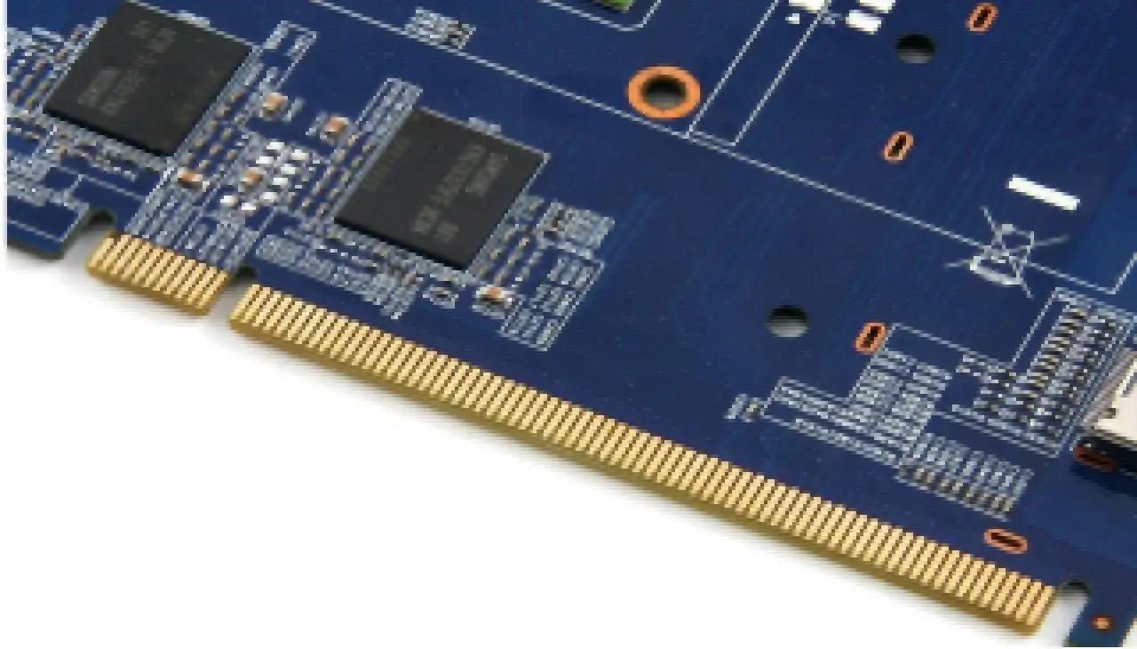
1. BasIC Chamfer Parameters
| Item | Requirement | Inspection Method |
|---|---|---|
| Chamfer Angle | 30° or 45° (±2° tolerance) | Projector/Optical Profilometer |
| Chamfer Length | 0.2–0.5mm (±0.1mm tolerance) | Micrometer/Laser Scan |
| Symmetry | Bilateral length difference ≤0.05mm | CMM (Coordinate Measuring Machine) |
2. Cosmetic Defect Control
-
Plating Integrity:
-
No copper exposure or gold peeling (Au thickness ≥0.8μm, Ni underlayer 3–5μm).
-
SCRatch depth ≤5μm (no visible cracks under 100× microscope).
-
-
Edge Quality:
-
Burr-free and chipping-free (smooth touch, fiber residue width <20μm).
-
Smooth transition between chamfer and PCB suRFace (R-angle ≤0.1mm).
-
3. Dimensional & Geometric Tolerances
| Key Item | Tolerance | Tool |
|---|---|---|
| Position Accuracy | ±0.15mm (relative to board edge) | 2D Image Measurer |
| Edge Perpendicularity | ≤0.1mm/100mm length | Square Gauge + Feeler Gauge |
| Coplanarity | Height variation ≤0.1mm across all fingers | Flatness Tester |
4. Functional Validation
-
Insertion Durability:
-
After 500 mating cycles, plating wear area <5%, contact resistance change ≤10%.
-
-
Environmental Reliability:
-
No plating cracks/delamination after thermal cycling (-40°C~+125°C, 100 cycles).
-
Edge corrosion depth ≤3μm after salt spray test (96hrs, 5% NaCl).
-
5. Process Defect Criteria
| Defect Type | Acceptance Criteria | Rejection Criteria |
|---|---|---|
| Angle Deviation | ≤±2° | >±3° or functional impairment |
| Plating Voids | Single void ≤0.1mm, ≤2 voids total | Exposed base material or continuous voids |
| Mechanical Damage | Chip depth ≤0.05mm | Causing impedance shift or short circuit |