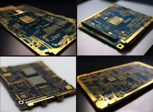
 PCB
PCB FPC
FPC Rigid-Flex
 FR-4
FR-4 HDI PCB
 Rogers High-Frequency Board
 PTFE Teflon High-Frequency Board
 Aluminum
 Copper Core
 PCB Assembly
 LED light PCBA
 Memory PCBA
 Power Supply PCBA
 New Energey PCBA
 Communication PCBA
 Industrial Control PCBA
 Medical Equipment PCBA
 Testing Service
 PCBA Testing Service
 Certification Application
 RoHS Certification Application
 REACH Certification Application
 CE Certification Application
 FCC Certification Application
 CQC Certification Application
 UL Certification Application
 Transformers, Inductors
 High Frequency Transformers
 Low Frequency Transformers
 High Power Transformers
 Conversion Transformers
 Sealed Transformers
 Ring Transformers
 Inductors
 Wires,Cables Customized
 Network Cables
 Power Cords
 Antenna Cables
 Coaxial Cables
 Net Position Indicator
 Solar AIS net position indicator
 Capacitors
 Connectors
 Diodes
 Embedded Processors & Controllers
 Digital Signal Processors (DSP/DSC)
 Microcontrollers (MCU/MPU/SOC)
 Programmable Logic Device(CPLD/FPGA)
 Communication Modules/IoT
 Resistors
 Through Hole Resistors
 Resistor Networks, Arrays
 Potentiometers,Variable Resistors
 Aluminum Case,Porcelain Tube Resistance
 Current Sense Resistors,Shunt Resistors
 Switches
 Transistors
 Power Modules
 Isolated Power Modules
 AC-DC Power Modules
 DC-AC Module(Inverter)
 RF and Wireless
Achieving Precision Plating Resist in Selective ENIG Process for 50μm-Pitch Areas
Selective Electroless Nickel Immersion Gold (ENIG) in advanced IC substrates and Hdi Pcbs requires defect-free plating resist patterning within 50μm pitch. The micron-scale accuracy and chemical resistance of the resist layer determine pad-line insulation reliability.
1. Plating Resist Materials and Coating
1.1 High-Resolution Resist Materials
| Material | Resolution Limit | Chemical Resistance (80℃×10min) | Thickness |
|---|---|---|---|
| Liquid Photo Resist (LPR) | 20μm | Slight swelling (<5%) | 8-10μm |
| Dry Film Resist (DFR) | 35μm | No swelling | 15-20μm |
| Laser Thermal Layer (LTHC) | 5μm | Fully inert | 2-3μm |
1.2 Coating Process Optimization
-
Spin coating (LPR):
-
Step 1: 500rpm×10s (spread);
-
Step 2: 2000rpm×30s (uniform film), thickness CV≤3%;
-
-
Lamination (DFR):
-
Temperature: 70±2℃;
-
Pressure: 0.4MPa;
-
Speed: 0.8m/min (bubble-free).
-
2. High-Precision Patterning
2.1 Exposure & Development
-
Exposure energy:
-
i-line (365nm): 120mJ/cm² (LPR);
-
Laser direct write (405nm): 25mW×50μm spot (LTHC);
-
-
Development:
-
1wt% Na₂CO₃, 0.15MPa spray, 60s;
-
Linewidth loss <5%, sidewall angle 85°±2° (Figure 1).
-
2.2 Edge Enhancement
-
Plasma ashing: O₂/N₂ (3:1), 300W×30s removes residues;
-
Micro-etching: H₂SO₄-Na₂S₂O₈ (pH=2), 0.2-0.5μm depth for adhesion.
3. Selective ENIG Process
3.1 Electroless Ni/Au Parameters
| Parameter | Ni Layer (EN) | Au Layer (IG) |
|---|---|---|
| Temperature | 85±0.5℃ | 88±0.5℃ |
| pH | 4.5-5.0 | 6.0-6.5 |
| Deposition Rate | 15μm/h | 0.05μm/min |
| Additives | Stabilizer (thiourea) | Complexant (citrate) |
3.2 Anti-Overplating Measures
-
Electric shielding: Auxiliary cathodes reduce edge current density (Figure 2);
-
Pulse plating: 30% duty cycle, 100Hz suppresses dendrites;
-
Real-time monitoring: Hull cell tests maintain ±5% Ni²⁺ stability.
4. Inspection & Defect Analysis
4.1 In-line Monitoring
-
AOI: 5μm resolution detects overplating/pinholes;
-
XRF thickness: Ni (2-5μm), Au (0.05-0.1μm), ±0.01μm accuracy.
4.2 Defect Remediation
-
Overplating: Laser ablation (355nm, 0.5J/cm²);
-
Non-uniformity: Adjust spray angle to 30°, flow rate to 2m/s.
5. Case Studies & Validation
5.1 5G mmWave Antenna Module
-
Design:
-
Pitch: 50μm;
-
Pad size: 80×80μm²;
-
-
Results:
Metric Before After Overplating Rate 12% 0.3% Insulation (1GHz) 10⁸Ω 10¹²Ω Thickness Uniformity ±15% ±5%
5.2 Reliability Tests
-
Thermal stress: 260℃ reflow ×3 cycles, no delamination;
-
Chemical resistance: 15min ENIG bath, linewidth change <0.5μm.