 PCB
PCB FPC
FPC Rigid-Flex
 FR-4
FR-4 HDI PCB
 Rogers High-Frequency Board
 PTFE Teflon High-Frequency Board
 Aluminum
 Copper Core
 PCB Assembly
 LED light PCBA
 Memory PCBA
 Power Supply PCBA
 New Energey PCBA
 Communication PCBA
 Industrial Control PCBA
 Medical Equipment PCBA
 Testing Service
 PCBA Testing Service
 Certification Application
 RoHS Certification Application
 REACH Certification Application
 CE Certification Application
 FCC Certification Application
 CQC Certification Application
 UL Certification Application
 Transformers, Inductors
 High Frequency Transformers
 Low Frequency Transformers
 High Power Transformers
 Conversion Transformers
 Sealed Transformers
 Ring Transformers
 Inductors
 Wires,Cables Customized
 Network Cables
 Power Cords
 Antenna Cables
 Coaxial Cables
 Net Position Indicator
 Solar AIS net position indicator
 Capacitors
 Connectors
 Diodes
 Embedded Processors & Controllers
 Digital Signal Processors (DSP/DSC)
 Microcontrollers (MCU/MPU/SOC)
 Programmable Logic Device(CPLD/FPGA)
 Communication Modules/IoT
 Resistors
 Through Hole Resistors
 Resistor Networks, Arrays
 Potentiometers,Variable Resistors
 Aluminum Case,Porcelain Tube Resistance
 Current Sense Resistors,Shunt Resistors
 Switches
 Transistors
 Power Modules
 Isolated Power Modules
 AC-DC Power Modules
 DC-AC Module(Inverter)
 RF and Wireless
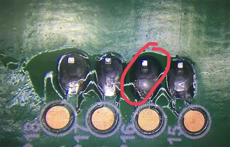
Detailed Explanation of Criteria and Acceptable Range for Common Solder Joint Voids (< 5% Area)
2025-09-02
1. BasIC Understanding: Definition and Core Impacts of Solder Joint Voids
Solder joint voids refer to cavities formed inside solder due to incomplete discharge of air and flux volatile gases during the soldering process. Typically, the "percentage of void area relative to the total solder joint area" is used as a quantitative indicator.
Voids are not completely prohibited—tiny voids with an area < 5% have minimal impact on the mechanical strength (tensile/shear strength) and electrical conductivity of solder joints (with a reduction of < 3%), and are regarded as "acceptable defects" in the industry. However, strict judgment standards must be followed: only tiny voids of specific types and in specific locations are permitted, and they must meet the prerequisite of "not affecting the core function of the solder joint." The core reference standard is IPC-A-610 (Acceptability of Electronic Assemblies), and the judgment requirements for voids are highly consistent across different versions (e.g., Rev G, Rev H), making it a globally recognized core basis.
2. Core Judgment Standards: General Rules for Voids with Area < 5%
Regardless of the component type, voids with an area < 5% must first meet the following 3 general judgment criteria before being evaluated for "acceptable range":
- Accuracy of Area Calculation:
Measurements must be conducted using "2D cross-sectional microscopic observation" (e.g., metallographic microscope) or "3D X-ray inspection" (for hidden solder joints such as BGA/CSP). The void area is calculated as the length × width of a single void (for irregular voids, estimation is based on the "minimum enclosing rectangle"), and the total solder joint area refers to the actual soldering area of the solder joint (e.g., the pad area for chip Resistor solder joints, and the projected area of solder balls for BGA solder joints). The calculation results must be accurate to 0.1% (to avoid misjudgment due to measurement errors). - Void Location Restrictions:
Voids are prohibited in the "solder joint functional area"—such as the "pin-pad contact area" of chip components, the "central conductive area" of BGA solder balls, and the "solder-wrapped section" of through-hole component pins. They are only allowed in the "non-functional area" (e.g., the edge of chip solder joints, the periphery of BGA solder balls) and must be at least 0.1mm away from the functional area (to prevent void expansion from affecting conductivity). - Void Quantity Restrictions:
Within a single solder joint, the number of voids with an area < 5% must be ≤ 2 (for circular voids, the diameter must be ≤ 0.2mm). For multiple tiny voids (e.g., more than 3, each with an area < 2%), the "total void area must be ≤ 5%" and "there must be no adjacent voids (with a spacing ≥ 0.1mm)" to avoid voids overlapping to form "hidden large voids" (with a total area exceeding 5%).
3. Acceptable Ranges for Voids with Area < 5% by Component Type
The solder joint structure and functional requirements vary significantly among different components. The acceptable range for voids with an area < 5% must be adjusted based on component characteristics, with the core classifications as follows:
1. Chip Components (0402-1206 Resistors/Capacitors, SOT Package Transistors)
- Solder Joint Structure: The solder joint is a rectangular or circular contact area between the "pad and component terminal electrode" (usually with an area of 0.1-0.5mm²), whose function is to achieve electrical connection and mechanical fixation (no high-density pin requirements).
- Acceptable Range:
- The void area is < 5%, and must meet: ① The void does not cover the "core contact area" of the component terminal electrode (accounting for more than 70% of the terminal electrode area to ensure current path); ② The number of voids in a single solder joint is ≤ 2, with no continuous distribution (e.g., 2 small voids evenly distributed along the pad edge, each with an area of 3%, are acceptable).
- Example: For an 0805 resistor with a pad area of 0.2mm² (length 0.5mm × width 0.4mm), a single void with an area ≤ 0.01mm² (5% × 0.2mm²) located at the pad edge (not covering the contact center between the resistor terminal electrode and the pad) is judged as acceptable.
- Prohibited Situation: If a void covers the core contact area of the terminal electrode (e.g., a 4% area void in the center of the 0805 resistor terminal electrode), it is judged as unacceptable even if the area is < 5% (as it may lead to an increase in contact resistance).
2. Fine-Pitch Chip Components (QFP, TQFP, Pin Pitch ≤ 0.5mm)
- Solder Joint Structure: The solder joint is an elongated strip-shaped area between the "pin and pad" (usually with a width of 0.2-0.3mm and a length of 0.4-0.6mm), whose function is to achieve high-density signal transmission (requiring avoidance of signal crosstalk and poor contact).
- Acceptable Range:
- The void area is < 5%, and must meet: ① The void does not "penetrate" along the length of the pin (i.e., the void length is < 50% of the pin solder joint length to avoid narrowing of the current path); ② There are no "corresponding voids" in the solder joints of adjacent pins (e.g., pins 1 and 2 each have a 3% void at the same position, which may cause signal crosstalk and is judged as unacceptable).
- Example: For a QFP with a pin pitch of 0.4mm and a solder joint area of 0.12mm² (length 0.5mm × width 0.24mm), a single void with an area ≤ 0.006mm² located at one end of the pin solder joint (length 0.2mm < 0.5mm × 50% = 0.25mm) is judged as acceptable.
- Special Requirement: For QFPs used in high-frequency signals (> 1GHz), even if the void area is < 5%, if it is located in the "signal transmission center area" of the pin solder joint (e.g., the middle position of the pin), it must be judged as unacceptable (as it may cause signal reflection).
3. BGA/CSP Components (Ball Grid Array/Chip Scale Package)
- Solder Joint Structure: The solder joint is a "solder ball" (with a diameter of 0.3-0.8mm), completely enclosed between the bottom of the component and the PCB pad. It is a "hidden solder joint" (requiring 3D X-ray inspection) and functions to achieve high-reliability interconnection (e.g., CPU, memory chips).
- Acceptable Range:
- The void area is < 5% (calculated based on the projected area of the solder ball), and must meet: ① The void is not located in the "central area" of the solder ball (the central diameter accounts for less than 50% of the solder ball diameter to ensure the core conductive path); ② Within the same component, the number of solder balls with voids is ≤ 10% of the total number of solder balls (e.g., for a 100-ball BGA, a maximum of 10 solder balls can have voids < 5%), and there are no "adjacent solder balls with voids" (spacing < 2 times the solder ball diameter).
- Example: For a BGA solder ball with a diameter of 0.5mm and a projected area of 0.196mm², a single void with an area ≤ 0.0098mm² located at the edge of the solder ball (distance from the center > 0.125mm) is judged as acceptable.
- Industry-Specific Specification: For BGAs used in automotive electronics and medical equipment, even if the void area is < 5%, the requirement is that "the number of solder balls with voids is ≤ 5%" (stricter than the general standard) to ensure reliability in extreme environments.
4. Through-Hole Components (DIP Chips, Connectors, Power Resistors)
- Solder Joint Structure: The solder joint is a cylindrical area between the "pin and pad hole" (solder wraps around the pin, with a height of 1.0-1.5mm), whose function is to achieve mechanical fixation and high-current transmission (e.g., power pins).
- Acceptable Range:
- The void area is < 5% (calculated based on the cross-sectional area of the solder joint; the cross-section is an annulus, with area = π(R² - r²), where R is the radius of the pad hole and r is the radius of the pin), and must meet: ① The void does not "continuously distribute" along the axial direction of the pin (i.e., the void height is < 30% of the solder joint height to avoid a decrease in mechanical strength); ② The void area of solder joints for power pins (carrying current > 1A) is < 3% (stricter than that for signal pins) to prevent overheating at the void due to excessive current.
- Example: For a DIP chip pin with a diameter of 0.6mm, a pad hole diameter of 0.8mm, and a solder joint cross-sectional area of 0.219mm², a single void with an area ≤ 0.011mm² and a height of 0.2mm < 1.5mm × 30% = 0.45mm is judged as acceptable.
- Prohibited Situation: A solder joint of a through-hole power resistor (carrying 2A current) with a 4% area void is judged as unacceptable even if it is < 5% (as it may cause the solder at the void to melt due to excessive current density).
4. Judgment Process and Common Misunderstandings
1. Standardized Judgment Process (Ensuring No Omissions)
- Step 1: Determine the Inspection Method: Use 2D microscopic observation for chip components, 3D X-ray for BGA/CSP, and cross-sectional slicing observation for through-hole components.
- Step 2: Measurement and Calculation: Determine the total solder joint area, the area and quantity of individual voids, and calculate the void ratio.
- Step 3: Location Verification: Check whether the void is located in the functional area and whether it meets the location restrictions of the component type.
- Step 4: Quantity Verification: Confirm the number and distribution of voids (whether they are adjacent, whether they exceed the proportion of total solder balls).
- Step 5: Comprehensive Judgment: If all general rules and component-specific requirements are met, judge as "acceptable"; if any condition is not met, judge as "unacceptable."
2. Common Misunderstandings and Avoidance Methods
- Misunderstanding 1: Judging Only by Area, Ignoring Location
Consequence: A 4% void located in the center of a BGA solder ball is misjudged as acceptable, leading to poor conductivity later.
Avoidance: Always check the void location first; voids with 不合格 locations must be rejected even if their area is < 5%. - Misunderstanding 2: Replacing Accurate Measurement with "Visual Estimation"
Consequence: The error of visual estimation for void area can reach ±3% (e.g., an actual 6% void is misjudged as 4%).
Avoidance: Measuring tools (e.g., area measurement functions of microscopes, X-ray inspection software) must be used, with accuracy to 0.1%. - Misunderstanding 3: Ignoring the "Total Void Area" Restriction
Consequence: A single BGA solder ball with 3 voids of 2% each (total area 6%) is misjudged as acceptable because each individual area is < 5%.
Avoidance: Both the "area of individual voids" and "total void area" must be calculated, and both must be < 5%.
5. Conclusion: Core Acceptability Principles for Voids with Area < 5%
The acceptable range for common solder joint voids (area < 5%) essentially lies in "not affecting the core functions of the solder joint (conductivity, mechanical fixation)," which can be summarized into 3 principles:
- Location Priority: Voids are prohibited in functional areas (e.g., contact centers, signal transmission areas) and only allowed in non-functional areas.
- Quantitative Control: The area of individual voids is < 5%, the total void area is < 5%, and the quantity and distribution comply with component restrictions.
- Scenario Adaptation: For high-reliability scenarios (automotive, medical) and high-current/high-frequency scenarios, the acceptable range must be further narrowed (e.g., area < 3%, quantity < 5%).
Solder joint voids with an area less than 5% are generally acceptable for all product classes if they are located in the center or interior of the joint, are not clustered, and do not involve any connection interfaces. However, the location of a void is more important than its size. When defining the final criteria, the product's end-use, specific customer requirements, and potential reliability risks should always be prioritized.