 PCB
PCB FPC
FPC Rigid-Flex
 FR-4
FR-4 HDI PCB
 Rogers High-Frequency Board
 PTFE Teflon High-Frequency Board
 Aluminum
 Copper Core
 PCB Assembly
 LED light PCBA
 Memory PCBA
 Power Supply PCBA
 New Energey PCBA
 Communication PCBA
 Industrial Control PCBA
 Medical Equipment PCBA
 Testing Service
 PCBA Testing Service
 Certification Application
 RoHS Certification Application
 REACH Certification Application
 CE Certification Application
 FCC Certification Application
 CQC Certification Application
 UL Certification Application
 Transformers, Inductors
 High Frequency Transformers
 Low Frequency Transformers
 High Power Transformers
 Conversion Transformers
 Sealed Transformers
 Ring Transformers
 Inductors
 Wires,Cables Customized
 Network Cables
 Power Cords
 Antenna Cables
 Coaxial Cables
 Net Position Indicator
 Solar AIS net position indicator
 Capacitors
 Connectors
 Diodes
 Embedded Processors & Controllers
 Digital Signal Processors (DSP/DSC)
 Microcontrollers (MCU/MPU/SOC)
 Programmable Logic Device(CPLD/FPGA)
 Communication Modules/IoT
 Resistors
 Through Hole Resistors
 Resistor Networks, Arrays
 Potentiometers,Variable Resistors
 Aluminum Case,Porcelain Tube Resistance
 Current Sense Resistors,Shunt Resistors
 Switches
 Transistors
 Power Modules
 Isolated Power Modules
 AC-DC Power Modules
 DC-AC Module(Inverter)
 RF and Wireless
The photochemical methods for pattern transfer in PCB manufacturing
The photochemICal methods for pattern transfer in PCB manufacturing mainly include photochemical etching, liquid photo - resist method, and dry film photoresist method. The following is a detailed introduction:
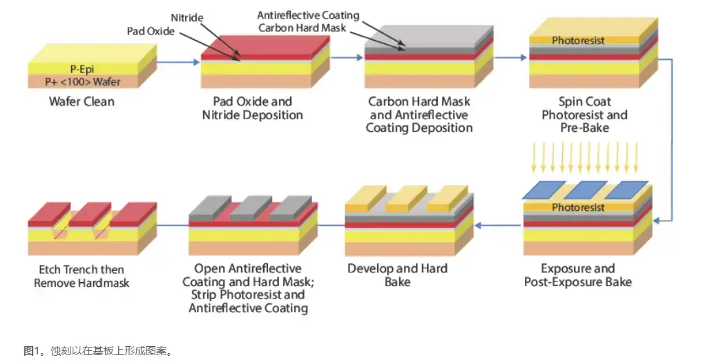
Photochemical Etching Method
1、Coating Photoresist: Evenly coat the photosensitive resist on the copper layer suRFace of the copper - clad laminate. The photosensitive resist is a chemical substance sensitive to light, which will undergo a chemical reaction under light irradiation.
2、Exposure: Make the designed circuit pattern into a negative film. Then, put the negative film and the copper - clad laminate coated with photoresist into an exposure machine, and expose them to light sources such as ultraviolet light. During the exposure process, the photoresist corresponding to the transparent part of the negative film will be irradiated by light and undergo a photochemical reaction, while the part of the photoresist blocked by the negative film will not react.
3、Development: Put the exposed copper - clad laminate into the developer. The unexposed photoresist will be dissolved and removed by the developer, so that the part of the copper layer that needs to be etched is exposed, forming an anti - etch pattern corresponding to the circuit pattern.
4、Etching: Immerse the developed copper - clad laminate in the etchant. The copper layer not protected by the photoresist will be dissolved by the etchant, while the part covered by the photoresist will be retained, thus forming the required circuit pattern.
5、Stripping: After etching, use a special stripping solution to remove the remaining photoresist, leaving only the copper circuit lines on the surface of the Circuit Board.
Liquid Photo - resist Method
1、Coating Liquid Photo - resist: Apply the liquid photo - resist evenly on the surface of the copper - clad laminate by spraying, rolling, or dipping. The liquid photo - resist is composed of photosensitive resin, photosensitizer, colorant, filler, and solvent, and it belongs to the negative - type photosensitive polymerization.
2、Exposure: Tightly fit the coated copper - clad laminate with the film carrying the circuit pattern and put it into the exposure equipment for exposure. Under the irradiation of light sources such as ultraviolet light, the photosensitive resin in the liquid photo - resist undergoes a photopolymerization reaction.
3、Development: Put the exposed copper - clad laminate into the developer. The unexposed part of the liquid photo - resist will be dissolved and removed by the developer, while the exposed and polymerized part will be retained, forming an anti - etch layer of the circuit pattern.
4、Subsequent Processing: After processes such as etching and cleaning, remove the copper foil not protected by the anti - etch layer, and finally obtain the PCB with the required circuit pattern.
Dry Film Photoresist Method
1、Lamination: Attach the dry film photoresist to the copper surface of the copper - clad laminate through a laminator. The dry film photoresist is a pre - coated film with photoresist, usually composed of a polyester film, a photoresist layer, and a release layer.
2、Exposure: Expose the copper - clad laminate with the attached dry film photoresist together with the film of the circuit pattern. Use ultraviolet light to make the photosensitive components in the dry film photoresist undergo a polymerization reaction, forming a cross - linked structure corresponding to the pattern.
3、Development: Treat the exposed copper - clad laminate with the developer. The unexposed dry film photoresist will be dissolved and carried away by the developer, while the exposed and polymerized part will be retained, forming an anti - etch pattern on the copper foil surface.
4、Etching and Stripping: Similar to the photochemical etching method, carry out the etching operation to remove the unnecessary copper foil, and then use the stripping agent to remove the dry film photoresist to complete the pattern transfer.