 PCB
PCB FPC
FPC Rigid-Flex
 FR-4
FR-4 HDI PCB
 Rogers High-Frequency Board
 PTFE Teflon High-Frequency Board
 Aluminum
 Copper Core
 PCB Assembly
 LED light PCBA
 Memory PCBA
 Power Supply PCBA
 New Energey PCBA
 Communication PCBA
 Industrial Control PCBA
 Medical Equipment PCBA
 Testing Service
 PCBA Testing Service
 Certification Application
 RoHS Certification Application
 REACH Certification Application
 CE Certification Application
 FCC Certification Application
 CQC Certification Application
 UL Certification Application
 Transformers, Inductors
 High Frequency Transformers
 Low Frequency Transformers
 High Power Transformers
 Conversion Transformers
 Sealed Transformers
 Ring Transformers
 Inductors
 Wires,Cables Customized
 Network Cables
 Power Cords
 Antenna Cables
 Coaxial Cables
 Net Position Indicator
 Solar AIS net position indicator
 Capacitors
 Connectors
 Diodes
 Embedded Processors & Controllers
 Digital Signal Processors (DSP/DSC)
 Microcontrollers (MCU/MPU/SOC)
 Programmable Logic Device(CPLD/FPGA)
 Communication Modules/IoT
 Resistors
 Through Hole Resistors
 Resistor Networks, Arrays
 Potentiometers,Variable Resistors
 Aluminum Case,Porcelain Tube Resistance
 Current Sense Resistors,Shunt Resistors
 Switches
 Transistors
 Power Modules
 Isolated Power Modules
 AC-DC Power Modules
 DC-AC Module(Inverter)
 RF and Wireless
Analysis of Insufficient Solder Fillet Height on Through-Hole Component Leads After Wave Soldering: Flux Activity vs. Wave Height/Contact Time
2026-01-08
Wave soldering has long been a cornerstone process in the electronics manufacturing industry, particularly for assembling printed Circuit Boards (PCBs) with through-hole components (THCs). It enables mass production with high efficiency and relatively low cost, making it indispensable for various electronic products ranging from consumer electronics to industrial control systems. A critical quality criterion in wave soldering is the solder fillet height on THC leads. Sufficient solder fillet height not only ensures reliable electrical conductivity between components and the PCB but also provides mechanical stability, resisting vibration, thermal cycling, and other environmental stresses during the product's lifecycle. However, insufficient solder fillet height is one of the most common defects encountered in wave soldering processes, leading to potential field failures, increased rework costs, and compromised product reliability.
When addressing insufficient solder fillet height on through-hole component leads, two factors are frequently identified as primary suspects: inadequate flux activity and improper wave height/contact time. Flux plays a vital role in the soldering process by removing oxides from the component leads and PCB pads, preventing reoxidation during heating, and reducing the suRFace tension of the molten solder to facilitate wetting and spreading. Meanwhile, wave height and contact time directly determine the amount of molten solder available for forming the fillet and the duration of interaction between the solder wave and the PCB/leads. Distinguishing between these two causes is essential for implementing targeted process improvements and eliminating the defect effectively.
This article aims to conduct a comprehensive analysis of insufficient solder fillet height on through-hole component leads after wave soldering, focusing on comparing and distinguishing the effects of flux activity insufficiency and improper wave height/contact time. It will first elaborate on the theoretical basis of wave soldering and the formation mechanism of solder fillets for through-hole components. Subsequently, it will respectively explore how insufficient flux activity and improper wave height/contact time lead to insufficient solder fillet height, including their respective failure mechanisms, characteristic defects, and influencing factors. Furthermore, this article will provide methods for differentiating these two causes through practical testing and observation, and summarize corresponding process optimization strategies. Finally, it will discuss other potential factors that may contribute to the defect to ensure a comprehensive understanding of the problem.
1. Theoretical Basis of Wave Soldering and Solder Fillet Formation for Through-Hole Components
To accurately analyze the causes of insufficient solder fillet height, it is necessary to first clarify the basic principles of the wave soldering process and the formation mechanism of solder fillets for through-hole components. This provides a theoretical framework for understanding how various process parameters affect the final soldering quality.
1.1 Overview of the Wave Soldering Process
The wave soldering process typically consists of several sequential stages: PCB preheating, flux application, wave soldering, and cooling. First, the PCB with mounted through-hole components is conveyed into the preheating zone. Preheating raises the temperature of the PCB and components gradually, which helps to evaporate the solvent in the flux, activate the flux in advance, and reduce the thermal shock experienced by the PCB and components when they come into contact with the high-temperature molten solder. Next, the preheated PCB passes through the flux application system, where flux is uniformly applied to the bottom surface of the PCB (the side to be soldered). The flux-coated PCB then enters the wave soldering zone, where it comes into contact with one or more molten solder waves. The molten solder wets the component leads and PCB pads, forms solder joints, and fills the through-holes. Finally, the soldered PCB moves to the cooling zone, where the molten solder solidifies rapidly to form stable solder joints.
The core of the wave soldering process lies in the interaction between the molten solder wave and the PCB/through-hole components. The solder wave is generated by a pump that drives the molten solder (usually Sn-Pb or lead-free alloys such as SAC305) through a nozzle, forming a continuous and stable wave. The key parameters in this stage include wave height, contact time between the PCB and the solder wave, conveyor speed, and soldering temperature. These parameters, together with flux properties, directly determine the quality of the solder joints.
1.2 Formation Mechanism of Solder Fillets for Through-Hole Components
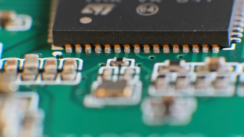
For through-hole components, the ideal solder joint should have the molten solder fill the through-hole completely or partially, and form a smooth, concave solder fillet on both the top and bottom surfaces of the PCB. The solder fillet height is defined as the vertical distance from the edge of the PCB pad to the highest point of the solder fillet on the component lead. The formation of the solder fillet is a result of the combined action of wetting, spreading, and capillary forces.
First, the flux must effectively remove the oxide layers on the surface of the component leads (usually made of copper or copper alloys) and the PCB pads. Oxides act as barriers that prevent the molten solder from wetting the metal surfaces. After oxide removal, the molten solder comes into direct contact with the clean metal surfaces, and wetting occurs due to the reduction of surface tension. Wetting is a prerequisite for solder fillet formation; without adequate wetting, the solder will not spread on the leads and pads but will form discrete droplets, resulting in poor solder joints.
Subsequently, the molten solder spreads along the component leads and PCB pads under the action of surface tension. At the same time, capillary force drives the molten solder to rise in the through-hole, filling the gap between the lead and the hole wall. The amount of solder that rises in the through-hole and the height of the solder fillet formed on the surface depend on the balance between capillary force, surface tension of the solder, and the gravitational force acting on the molten solder. When the PCB leaves the solder wave, the molten solder attached to the leads and pads solidifies, forming the final solder fillet. The height of this fillet is a direct reflection of the adequacy of the soldering process: insufficient height indicates that the solder did not wet and spread properly, or that there was an insufficient amount of solder available for fillet formation.
2. Insufficient Flux Activity: Mechanism and Effects on Solder Fillet Height
Flux is an essential auxiliary material in wave soldering, and its activity directly affects the wetting and spreading of molten solder. Insufficient flux activity is a common cause of insufficient solder fillet height on through-hole component leads. This section will elaborate on the role of flux, the causes of insufficient activity, and how this insufficiency leads to the defect.
2.1 The Role of Flux in Wave Soldering
Flux performs three core functions in the wave soldering process: oxide removal, anti-reoxidation, and surface tension reduction. First, oxide removal is the most critical function. During the manufacturing, storage, and preheating stages, component leads and PCB pads are easily oxidized in the air, forming a thin oxide layer (e.g., CuO, Cu₂O for copper leads). This oxide layer is chemically stable and has high electrical resistance, which prevents the molten solder from wetting the metal surface. Flux contains active ingredients (such as rosin derivatives, organic acids, or halides) that react with the oxide layer at elevated temperatures, converting the insoluble oxides into soluble compounds that can be washed away or left as a harmless residue. Second, flux forms a protective film on the cleaned metal surfaces during the soldering process, preventing reoxidation by isolating the surfaces from the air. Finally, flux reduces the surface tension of the molten solder, which promotes the spreading of the solder on the metal surfaces and enhances the capillary action that drives the solder into the through-holes.
The activity of flux is determined by the type and concentration of its active ingredients, as well as its activation temperature range. Flux can be classified into low-activity (R-type), medium-activity (RMA-type), and high-activity (RA-type) based on its activity level. Different soldering applications require flux with appropriate activity; for example, through-hole components with heavily oxidized leads or PCBs stored in harsh environments may require high-activity flux to ensure effective oxide removal.
2.2 Causes of Insufficient Flux Activity
Insufficient flux activity can be attributed to several factors, including improper flux selection, flux degradation, incorrect flux application, and inappropriate preheating parameters.
First, improper flux selection is a fundamental cause. If the flux's activity level is not matched to the degree of oxidation of the component leads or PCB pads, it will fail to remove oxides effectively. For example, using low-activity R-type flux for components with heavily oxidized leads will result in incomplete oxide removal, leading to poor wetting. Additionally, the activation temperature range of the flux must match the preheating and soldering temperatures. If the flux's activation temperature is higher than the preheating temperature but lower than the soldering temperature, it may not be fully activated before coming into contact with the molten solder, reducing its effectiveness.
Second, flux degradation can occur during storage or use. Flux has a limited shelf life; if stored beyond the expiration date, its active ingredients may decompose or react with moisture and air, reducing activity. During use, flux is often diluted with solvents to maintain the appropriate viscosity for application. If the dilution ratio is too high, the concentration of active ingredients will decrease, leading to insufficient activity. Moreover, if the flux application system is contaminated (e.g., with solder dross, dust, or moisture), the active ingredients may be consumed or inactivated.
Third, incorrect flux application can result in insufficient flux coverage or uneven distribution. If the flux coating on the PCB pads or component leads is too thin, there will not be enough active ingredients to remove oxides completely. Conversely, an excessively thick flux coating may trap solvents, which can evaporate violently during soldering, causing solder splashing and incomplete wetting. Uneven flux distribution (e.g., missing flux on some pads) will lead to localized insufficient activity, resulting in uneven solder fillet height.
Fourth, inappropriate preheating parameters can affect flux activation. Preheating is essential for evaporating the solvent in the flux and activating the active ingredients. If the preheating temperature is too low or the preheating time is too short, the solvent in the flux will not be fully evaporated, and the active ingredients will not be adequately activated. This leads to insufficient oxide removal and poor wetting. On the other hand, excessive preheating temperature or prolonged preheating time can cause the active ingredients of the flux to decompose or volatilize prematurely, reducing their activity before the soldering stage.
2.3 How Insufficient Flux Activity Leads to Insufficient Solder Fillet Height
Insufficient flux activity directly impairs the wetting and spreading of molten solder, which is the core mechanism leading to insufficient solder fillet height on through-hole component leads. The specific process can be divided into the following stages:
First, incomplete oxide removal. Due to insufficient activity, the flux fails to completely remove the oxide layers on the component leads and PCB pads. The remaining oxide layer acts as a barrier, preventing the molten solder from making direct contact with the clean metal surface. As a result, the wetting angle between the molten solder and the metal surface increases significantly (ideally, the wetting angle should be less than 90° for good soldering; a wetting angle greater than 90° indicates poor wetting). Poor wetting means that the molten solder cannot spread on the leads and pads but tends to form spherical droplets, which cannot form a continuous and sufficient solder fillet.
Second, reoxidation during soldering. Insufficient flux activity also means that the protective film formed by the flux is incomplete or unstable. During the soldering stage, the high-temperature molten solder causes the cleaned metal surfaces to reoxidize rapidly in the presence of air. The newly formed oxide layer further hinders wetting and spreading, exacerbating the problem of insufficient solder fillet height. In severe cases, the reoxidized surface may not be wetted by the solder at all, resulting in "non-wetting" defects, where the solder does not adhere to the leads or pads.
Third, reduced capillary action. The surface tension of the molten solder is not effectively reduced due to insufficient flux activity. High surface tension makes it difficult for the molten solder to be drawn into the through-hole by capillary force. As a result, the solder cannot rise sufficiently in the through-hole, and the solder fillet height on both the top and bottom surfaces of the PCB is insufficient. Even if some solder adheres to the leads, the fillet will be shallow and irregular, lacking the smooth, concave shape of a qualified solder joint.
Characteristic defects caused by insufficient flux activity include: uneven solder fillet height across multiple components (especially for components with similar oxidation levels), dull or rough solder fillet surfaces (due to incomplete wetting), presence of oxide inclusions in the solder fillet (visible under magnification), and localized non-wetting or dewetting (where the solder pulls away from the leads or pads). Additionally, these defects are often accompanied by excessive flux residue (if the flux is not fully activated or volatilized) or insufficient flux residue (if the flux was decomposed or volatilized prematurely).
3. Improper Wave Height/Contact Time: Mechanism and Effects on Solder Fillet Height
Wave height and contact time are key process parameters in the wave soldering stage, directly determining the amount of molten solder available for forming the solder fillet and the duration of interaction between the solder and the PCB/leads. Even if the flux activity is sufficient, improper wave height or contact time can still lead to insufficient solder fillet height. This section will explore the role of wave height and contact time, the causes of their improper setting, and their impact on solder fillet formation.
The Role of Wave Height and Contact Time in Wave Soldering
Wave height refers to the vertical distance from the top of the solder wave to the conveyor belt. It determines how much of the PCB and component leads are immersed in the molten solder. For through-hole components, the wave height must be sufficient to ensure that the molten solder can reach the through-holes and form a solder fillet on both the bottom and top surfaces of the PCB (or at least the required height on the bottom surface). Insufficient wave height will result in inadequate solder coverage, while excessive wave height may cause solder to splash onto the top surface of the PCB, contaminating components or forming bridging defects between adjacent leads.
Contact time refers to the duration during which a specific point on the PCB is in contact with the molten solder wave. It is determined by the conveyor speed and the length of the solder wave. Sufficient contact time is required to ensure that the flux has enough time to complete the oxide removal process, the molten solder has enough time to wet and spread on the leads and pads, and the capillary action has enough time to drive the solder into the through-holes. Insufficient contact time will result in incomplete wetting and insufficient solder filling, while excessive contact time may cause overheating of the PCB and components, leading to thermal damage, solder oxidation, or excessive flux volatilization.
The combination of wave height and contact time directly affects the total amount of solder that adheres to the component leads and PCB pads. A balance between these two parameters is essential for forming a solder fillet of the required height. For example, a slightly lower wave height can be compensated by a longer contact time (within a reasonable range) to ensure sufficient solder coverage, and vice versa.
Causes of Improper Wave Height and Contact Time
Improper wave height and contact time can be caused by incorrect parameter setting, equipment wear or malfunction, and variations in PCB or component dimensions.
First, incorrect parameter setting is the most common cause. During the process setup phase, if the wave height and contact time are not calibrated according to the specific requirements of the PCB and components, defects will occur. For example, when switching to a PCB with thicker through-holes or longer component leads, if the wave height is not increased accordingly, the solder may not be able to fill the through-holes sufficiently. Similarly, if the conveyor speed is increased to improve production efficiency without adjusting the wave length (to maintain contact time), the contact time will be shortened, leading to insufficient solder wetting and filling.
Second, equipment wear or malfunction can lead to unstable wave height or contact time. The solder pump in the wave soldering machine can wear out over time, resulting in reduced pump pressure and unstable wave height (e.g., wave height fluctuating during operation). The nozzle of the wave soldering machine can also become clogged with solder dross, which distorts the shape of the solder wave, leading to uneven contact between the wave and the PCB. Additionally, the conveyor belt may slip or run at an inconsistent speed, causing variations in contact time across different PCBs or even different areas of the same PCB.
Third, variations in PCB or component dimensions can make the pre-set wave height and contact time inappropriate. For example, if the PCB thickness varies beyond the specified tolerance, a fixed wave height may be insufficient for thicker PCBs (resulting in inadequate immersion) or excessive for thinner PCBs (resulting in solder splashing). Similarly, component leads with inconsistent lengths or diameters can affect the amount of solder required for fillet formation; if the wave height and contact time are not adjusted to accommodate these variations, some components will have insufficient solder fillet height.
How Improper Wave Height/Contact Time Leads to Insufficient Solder Fillet Height
Improper wave height and contact time affect solder fillet formation by altering the amount of available solder and the duration of the soldering interaction. The specific mechanisms for insufficient wave height and insufficient contact time are slightly different, but both lead to the same result: insufficient solder fillet height.
In the case of insufficient wave height: The molten solder wave does not immerse the PCB and component leads deeply enough. For through-hole components, the solder wave may only reach the bottom of the through-holes, failing to fill the holes or form a sufficient fillet on the top surface. Even on the bottom surface, the amount of solder available for forming the fillet is limited. The solder cannot spread upward along the leads to the required height, resulting in a shallow fillet. Additionally, insufficient wave height may cause the solder wave to break when it comes into contact with the PCB, leading to uneven solder coverage. Some areas may have no solder at all, while others have only a thin layer, resulting in inconsistent and insufficient fillet height.
In the case of insufficient contact time: Even if the wave height is sufficient, the short duration of interaction between the molten solder and the PCB/leads means that the soldering process cannot be completed fully. First, the flux does not have enough time to completely remove the oxides on the leads and pads. Although the flux activity may be sufficient, insufficient time prevents the chemical reaction between the flux and oxides from reaching completion, leading to incomplete oxide removal and poor wetting. Second, the molten solder does not have enough time to wet and spread on the leads and pads. The solder may start to wet the surface but does not have enough time to spread to form a sufficient fillet before the PCB leaves the solder wave. Third, capillary action cannot drive the solder into the through-holes effectively within a short contact time. The solder may only fill the lower part of the through-holes, resulting in insufficient fillet height on both the top and bottom surfaces.
Characteristic defects caused by improper wave height/contact time include: consistent insufficient solder fillet height across multiple components (if the parameter setting is incorrect for the entire batch), uneven fillet height across the PCB (if the wave height is unstable or the conveyor speed is inconsistent), and shallow but relatively smooth fillet surfaces (since the flux activity is sufficient, the wetting is relatively good where the solder does contact the leads). Additionally, insufficient wave height may be accompanied by "solder starvation" (visible gaps between the solder fillet and the through-hole), while insufficient contact time may be accompanied by incomplete filling of the through-holes (the solder does not rise to the expected height in the holes).
4. Differentiation Between Flux Activity Insufficiency and Wave Height/Contact Time Issues
Distinguishing between insufficient flux activity and improper wave height/contact time is crucial for targeted process improvement. This section provides practical methods for differentiation, including visual inspection, microscopic analysis, process parameter verification, and controlled experiments.
4.1 Visual Inspection and Microscopic Analysis
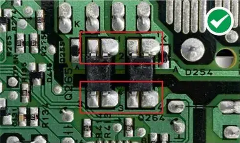
Visual inspection and microscopic analysis (using optical microscopes or electron microscopes) can reveal characteristic defects that help distinguish the two causes.
For defects caused by insufficient flux activity: As mentioned earlier, the solder fillets are often dull, rough, or irregular in shape. Under magnification, oxide inclusions can be observed in the solder fillet, and the interface between the solder and the lead/pad may be discontinuous (indicating incomplete wetting). Localized non-wetting or dewetting is common, and the defects may be more severe on components with heavily oxidized leads. Additionally, there may be excessive or abnormal flux residue (e.g., hard, brittle residue indicating incomplete activation, or sticky residue indicating unevaporated solvent).
For defects caused by improper wave height/contact time: The solder fillets are usually shallow but relatively smooth (if the flux activity is sufficient). Under magnification, the interface between the solder and the lead/pad is continuous (indicating good wetting where contact occurred), and there are no obvious oxide inclusions. The defects are often uniform across the PCB (e.g., all components have the same degree of insufficient fillet height) or consistent with the wave shape (e.g., defects concentrated in areas where the wave height was lowest). Solder starvation in the through-holes or incomplete filling is a typical sign of insufficient wave height, while insufficient contact time may result in fillets that are uniformly shallow but have a consistent shape.
4.2 Process Parameter Verification
Verifying the wave soldering process parameters is a direct method to determine if wave height or contact time is the cause.
Wave height verification: Use a wave height gauge to measure the actual wave height during operation. Compare the measured value with the specified process parameter. If the measured wave height is lower than the required value, or if the wave height fluctuates significantly (beyond the allowable range), insufficient wave height is likely the cause. Additionally, check the solder nozzle for clogging or damage, and the solder pump for wear or pressure instability, as these can affect wave height stability.
Contact time verification: Calculate the contact time based on the conveyor speed and the length of the solder wave (contact time = wave length / conveyor speed). Compare the calculated value with the specified process parameter. If the calculated contact time is shorter than the required value, insufficient contact time is a potential cause. Verify the conveyor speed using a tachometer to ensure it is consistent with the set value; speed fluctuations can also lead to inconsistent contact time.
If the wave height and contact time are within the specified ranges and stable, then the defect is more likely caused by insufficient flux activity or other factors.
4.3 Controlled Experiments
Controlled experiments can further confirm the cause by isolating the variables of flux activity and wave height/contact time.
Experiment 1: Test with increased flux activity. Keep the wave height and contact time unchanged, and replace the current flux with a higher-activity flux (or increase the concentration of the current flux by reducing the dilution ratio). If the solder fillet height improves significantly, the original defect was caused by insufficient flux activity. If there is no improvement, the cause is likely related to wave height/contact time or other factors.
Experiment 2: Test with adjusted wave height/contact time. Keep the flux type and application parameters unchanged. First, increase the wave height by a small increment (within the allowable range) and observe the effect on solder fillet height. If the height improves, insufficient wave height was the cause. If not, restore the wave height and increase the contact time (by reducing the conveyor speed or increasing the wave length) and observe. If the fillet height improves, insufficient contact time was the cause. If neither adjustment has an effect, the defect is likely due to insufficient flux activity or other factors (e.g., component lead oxidation, PCB pad contamination).
Experiment 3: Test with pre-cleaned components. If the defect is suspected to be due to insufficient flux activity caused by heavy lead oxidation, select a small number of components, pre-clean their leads with a suitable solvent (to remove oxides), and solder them under the original process parameters. If the solder fillet height of these components is normal, it confirms that the original flux activity was insufficient to remove the oxides on the leads.
5. Process Optimization Strategies for Improving Solder Fillet Height
Based on the identified cause (insufficient flux activity or improper wave height/contact time), targeted process optimization strategies can be implemented to improve the solder fillet height of through-hole components. This section summarizes the corresponding optimization measures for each cause.
5.1 Optimization Strategies for Insufficient Flux Activity
The core of optimizing for insufficient flux activity is to ensure that the flux can effectively remove oxides, prevent reoxidation, and reduce solder surface tension. The specific measures include:
First, select the appropriate flux. Based on the degree of oxidation of the component leads and PCB pads, choose a flux with matching activity. For components with heavily oxidized leads or PCBs stored in harsh environments, select high-activity RA-type flux. Ensure that the flux's activation temperature range matches the preheating and soldering temperatures; the flux should be fully activated before the PCB comes into contact with the molten solder.
Second, ensure proper flux storage and handling. Store flux in a sealed container in a cool, dry environment to prevent moisture absorption and active ingredient degradation. Use flux within its shelf life. When diluting flux, strictly follow the manufacturer's recommended dilution ratio to maintain the concentration of active ingredients. Regularly clean the flux application system (e.g., nozzles, tanks) to prevent contamination by solder dross, dust, or moisture.
Third, optimize flux application parameters. Adjust the flux application method (e.g., spray, foam, wave) and parameters to ensure uniform and sufficient flux coverage on the PCB pads and component leads. The flux coating thickness should be within the manufacturer's recommended range (usually 5-20 μm). For spray application, adjust the nozzle pressure and position to achieve uniform coverage; for foam application, adjust the air pressure to generate a stable, uniform foam layer.
Fourth, optimize preheating parameters. Adjust the preheating temperature and time to ensure that the solvent in the flux is fully evaporated and the active ingredients are fully activated. The preheating temperature should be set based on the flux's activation temperature; typically, the PCB bottom surface temperature before entering the solder wave should be 100-150°C for most fluxes. The preheating time should be sufficient to raise the PCB temperature gradually, avoiding thermal shock and ensuring uniform activation of the flux across the entire PCB.
5.2 Optimization Strategies for Improper Wave Height/Contact Time
The core of optimizing for improper wave height/contact time is to ensure that the molten solder wave fully immerses the PCB and component leads, and that the contact time is sufficient for complete wetting and filling. The specific measures include:
First, calibrate wave height accurately. Based on the PCB thickness, component lead length, and through-hole size, determine the appropriate wave height. The wave height should be sufficient to immerse the PCB bottom surface and the lower part of the through-holes, ensuring that the molten solder can rise into the through-holes by capillary action. Use a wave height gauge to calibrate the wave height regularly (e.g., at the start of each shift) and adjust the solder pump pressure as needed to maintain stable wave height. Regularly clean the solder nozzle to remove dross and ensure a smooth, stable wave shape.
Second, optimize contact time. Calculate the required contact time based on the flux activity, solder alloy, and component type (typically 2-5 seconds). Adjust the conveyor speed and wave length to achieve the required contact time. If the conveyor speed needs to be increased for production efficiency, increase the wave length accordingly to maintain contact time. Regularly verify the conveyor speed with a tachometer to ensure consistency and stability.
Third, address equipment wear and malfunction. Regularly inspect and maintain the wave soldering machine, including the solder pump, nozzle, conveyor belt, and drive system. Replace worn parts (e.g., pump impellers, conveyor belts) in a timely manner to ensure stable operation of the machine. Install wave height monitoring systems (if available) to detect and alert to wave height fluctuations in real time.
Fourth, control PCB and component dimensions. Work with suppliers to ensure that the PCB thickness, component lead length, and through-hole size are within the specified tolerances. Implement incoming inspection for PCBs and components to identify and reject non-conforming parts. For PCBs with slight thickness variations, adjust the wave height slightly for each batch to ensure sufficient immersion.
6. Other Potential Factors Affecting Solder Fillet Height
While insufficient flux activity and improper wave height/contact time are the primary causes of insufficient solder fillet height, other factors may also contribute to or exacerbate the defect. These factors should be considered during the troubleshooting process to ensure a comprehensive solution.
First, component lead and PCB pad contamination. In addition to oxidation, component leads and PCB pads may be contaminated with grease, oil, dust, or other impurities during manufacturing or handling. These contaminants can also prevent the flux from functioning effectively and the molten solder from wetting the surface. Even with sufficient flux activity and proper wave height/contact time, contamination can lead to insufficient solder fillet height. Incoming inspection and cleaning of components and PCBs can help mitigate this issue.
Second, soldering temperature. The soldering temperature (molten solder temperature) must be appropriate for the solder alloy and flux. If the temperature is too low, the molten solder has high viscosity, which reduces its fluidity and ability to wet and spread. This can lead to insufficient solder fillet height, even if flux activity and wave height/contact time are sufficient. If the temperature is too high, the solder may oxidize rapidly, forming dross that can contaminate the solder joints, and the flux may decompose prematurely, reducing its activity. The soldering temperature should be set based on the solder alloy's melting point (e.g., 245-255°C for SAC305 lead-free solder) and the manufacturer's recommendations.
Third, solder alloy composition and quality. The composition of the solder alloy affects its fluidity, wetting ability, and surface tension. For example, lead-free solder alloys (e.g., SAC305) have higher surface tension and lower fluidity compared to traditional Sn-Pb alloys, requiring higher flux activity and appropriate wave height/contact time to achieve sufficient solder fillet height. Contamination of the solder alloy (e.g., with excessive impurities) can also reduce its fluidity and wetting ability. Regularly test the solder alloy composition and remove dross from the solder pot to maintain solder quality.
Fourth, PCB design. Poor PCB design can also lead to insufficient solder fillet height. For example, overly small pad sizes, excessive through-hole diameters (relative to lead diameter), or insufficient pad spacing can affect the wetting and spreading of solder. Additionally, the presence of solder masks that cover part of the pads can reduce the available wetting area, leading to insufficient fillet height. Optimizing PCB design (e.g., appropriate pad size, through-hole diameter, and solder mask opening) can improve soldering quality.
Insufficient solder fillet height on through-hole component leads after wave soldering is a critical quality defect that can compromise the reliability of electronic products. The two primary causes of this defect are insufficient flux activity and improper wave height/contact time, each with distinct failure mechanisms and characteristic defects.
Insufficient flux activity impairs oxide removal, promotes reoxidation, and fails to reduce solder surface tension, leading to poor wetting and inadequate capillary action. This results in dull, irregular solder fillets with oxide inclusions and localized non-wetting. Improper wave height/contact time, on the other hand, limits the amount of available solder and the duration of the soldering interaction, leading to shallow but relatively smooth solder fillets, solder starvation, and incomplete through-hole filling.
Distinguishing between these two causes can be achieved through visual inspection, microscopic analysis, process parameter verification, and controlled experiments. Targeted process optimization strategies, such as selecting appropriate flux, optimizing flux application and preheating parameters, calibrating wave height, and adjusting contact time, can effectively improve solder fillet height.
Additionally, other factors such as component and PCB contamination, soldering temperature, solder alloy quality, and PCB design should be considered during troubleshooting to ensure a comprehensive solution. By systematically analyzing and optimizing the wave soldering process, manufacturers can eliminate insufficient solder fillet height defects, improve product reliability, and reduce rework costs.