 PCB
PCB FPC
FPC Rigid-Flex
 FR-4
FR-4 HDI PCB
 Rogers High-Frequency Board
 PTFE Teflon High-Frequency Board
 Aluminum
 Copper Core
 PCB Assembly
 LED light PCBA
 Memory PCBA
 Power Supply PCBA
 New Energey PCBA
 Communication PCBA
 Industrial Control PCBA
 Medical Equipment PCBA
 Testing Service
 PCBA Testing Service
 Certification Application
 RoHS Certification Application
 REACH Certification Application
 CE Certification Application
 FCC Certification Application
 CQC Certification Application
 UL Certification Application
 Transformers, Inductors
 High Frequency Transformers
 Low Frequency Transformers
 High Power Transformers
 Conversion Transformers
 Sealed Transformers
 Ring Transformers
 Inductors
 Wires,Cables Customized
 Network Cables
 Power Cords
 Antenna Cables
 Coaxial Cables
 Net Position Indicator
 Solar AIS net position indicator
 Capacitors
 Connectors
 Diodes
 Embedded Processors & Controllers
 Digital Signal Processors (DSP/DSC)
 Microcontrollers (MCU/MPU/SOC)
 Programmable Logic Device(CPLD/FPGA)
 Communication Modules/IoT
 Resistors
 Through Hole Resistors
 Resistor Networks, Arrays
 Potentiometers,Variable Resistors
 Aluminum Case,Porcelain Tube Resistance
 Current Sense Resistors,Shunt Resistors
 Switches
 Transistors
 Power Modules
 Isolated Power Modules
 AC-DC Power Modules
 DC-AC Module(Inverter)
 RF and Wireless
Wave Soldering Parameter Settings for Through-Hole Components
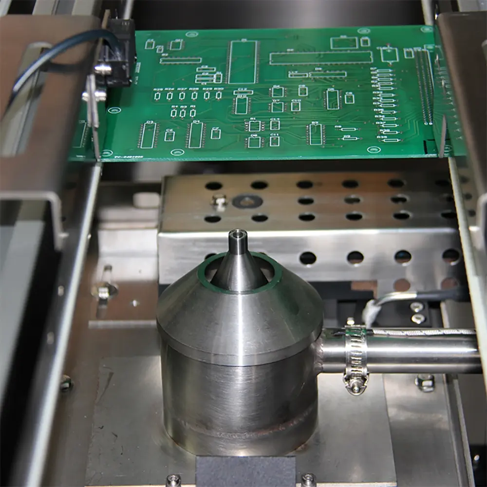
Abstract: Wave soldering parameters critICally impact joint reliability, hole fill rate, and component safety. Core parameters (preheat temperature, solder temperature, conveyor speed, tilt angle) must be dynamically adjusted based on PCB thickness, component thermal mass, and solder type. Per IPC-J-STD-001/610, typical settings are:
-
Solder Temp: 250±5°C (for lead-free SnAgCu)
-
Conveyor Speed: 1.5–2.0m/min (1.6mm board baseline)
-
Contact Time: 3–5 seconds
1. Key Parameter Settings
| Parameter | Standard Range | Formula/Adjustment Basis | Failure Risk |
|---|---|---|---|
| Preheat Temp | 90–110°C (double-side) | T_preheat = 0.8×T_melting + 20°C | Incomplete flux activation → ↑30% cold joints |
| Solder Temp | 250±5°C | T_solder = T_melting + 45±5°C | >260°C damages electrolytic Capacitors |
| Speed (V) | 1.5–2.0m/min | V = K × t_board(K=0.15×ln(Δt)) | Too fast → poor fill; too slow → carbonization |
| Tilt Angle (α) | 5–7° | α = arctan(h/100)(h: wave height) | <5° → ↑40% bridging risk |
| Contact Time (t) | 3–5 seconds | t = L_wave / V(L_wave: wave width) | <2s → fill rate <75% |
Note:
T_melting: Solder melting point (SnAgCu=217°C);
t_board: Thermal mass of thickest component (e.g., transformer t_board=8s).
2. Tiered Optimization Strategies
-
By PCB Thickness:
Thickness (mm) Speed (m/min) Preheat (°C) Principle 0.8–1.0 1.8–2.0 100–110 Thin boards: reduce speed to prevent overheating 1.6 (Baseline) 1.5–1.8 90–100 Balance fill rate & thermal stress ≥2.4 1.2–1.5 110–120 Thick boards: extend preheat time -
By Component Type:
-
Heatsinks/Transformers:
-
Preheat +10°C, contact time +2s (thermal mass compensation);
-
Add solder thieves (size=1.5× main pad).
-
-
Electrolytic Caps/Connectors:
-
Solder temp ↓ to 245°C (prevent seal rupture);
-
Wave height ↓20% (reduce impact force).
-
-
3. Process Window Validation
-
Temperature Profiling:
-
Attach K-type thermocouples to:
-
Ground copper (represents PCB bulk temp);
-
Component lead root (actual joint temp).
-
-
Pass Criteria:
-
Preheat slope 1–2°C/s;
-
Time above 220°C at lead root: 2.5–3.5s (IPC-610 7.4.2).
-
-
-
Solder Joint Quality:
Defect Class 3 Acceptance Root Cause Hole Fill ≥75% depth (cross-section) Insufficient preheat/speed Fillet Height 0.5–2.0mm Incorrect angle/wave height Bridging Zero tolerance (pitch<2.5mm) Flux failure/angle<5°
4. Failure Prevention & Dynamic Compensation
-
Real-Time Compensation Formulas:
-
Speed Correction: ΔV = -0.2 × (T_actual - 250)(Speed ↓0.2m/min per 1°C over 250°C)
-
Wave Height Correction: H_wave = 0.5 + 0.02 × t_board(mm)
-
-
Monitoring Tech:
-
IR Thermal Imager: Board surface ΔT <15°C;
-
Laser Profilometer: In-line fillet height check (±0.01mm).
-
5. Special Case Handling
-
Mixed Technology (SMT+THT):
-
Reflow SMT first, then wave solder THT;
-
3mm keepout zone around through-hole parts.
-
-
Selective Wave Soldering:
-
Local solder temp 260±5°C, nozzle speed 10mm/s;
-
Nitrogen cover (O₂ <100ppm) reduces dross.
-
Conclusion
Wave soldering requires "temperature-time-mechanics" balance:
-
Temperature: 250±5°C (lead-free), preheat 90–110°C (slope 1–2°C/s);
-
Time: Contact 3–5s (leads >220°C for 2.5–3.5s);
-
Mechanics: Speed 1.5–2.0m/min + tilt 5–7° + wave height 0.5–1mm.
Critical Controls:
-
Profile every 4 hours;
-
Increase parameters 10–20% for thick boards/large components;
-
Maintain Cu in solder bath ≤0.3% (add pure Sn if exceeded).