 PCB
PCB FPC
FPC Rigid-Flex
 FR-4
FR-4 HDI PCB
 Rogers High-Frequency Board
 PTFE Teflon High-Frequency Board
 Aluminum
 Copper Core
 PCB Assembly
 LED light PCBA
 Memory PCBA
 Power Supply PCBA
 New Energey PCBA
 Communication PCBA
 Industrial Control PCBA
 Medical Equipment PCBA
 Testing Service
 PCBA Testing Service
 Certification Application
 RoHS Certification Application
 REACH Certification Application
 CE Certification Application
 FCC Certification Application
 CQC Certification Application
 UL Certification Application
 Transformers, Inductors
 High Frequency Transformers
 Low Frequency Transformers
 High Power Transformers
 Conversion Transformers
 Sealed Transformers
 Ring Transformers
 Inductors
 Wires,Cables Customized
 Network Cables
 Power Cords
 Antenna Cables
 Coaxial Cables
 Net Position Indicator
 Solar AIS net position indicator
 Capacitors
 Connectors
 Diodes
 Embedded Processors & Controllers
 Digital Signal Processors (DSP/DSC)
 Microcontrollers (MCU/MPU/SOC)
 Programmable Logic Device(CPLD/FPGA)
 Communication Modules/IoT
 Resistors
 Through Hole Resistors
 Resistor Networks, Arrays
 Potentiometers,Variable Resistors
 Aluminum Case,Porcelain Tube Resistance
 Current Sense Resistors,Shunt Resistors
 Switches
 Transistors
 Power Modules
 Isolated Power Modules
 AC-DC Power Modules
 DC-AC Module(Inverter)
 RF and Wireless
The Impacts of Excessive Copper Content in Wave Soldering Solder Pots on Soldering Quality and Equipment
2025-12-24
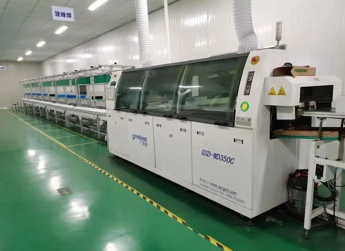
Wave soldering is a pivotal mass soldering process in printed circuit board assembly (PCBA) manufacturing, widely used for soldering through-hole components and suRFace-mount devices (SMDs) with gull-wing or J-lead configurations. The solder pot (tin furnace) is the core component of a wave soldering machine, holding molten solder alloy (typically Sn-Cu, Sn-Ag-Cu, or Sn-Pb) that forms the solder wave to wet and bond component leads to PCB pads. During normal operation, copper from PCB pads, component leads, and solder joints dissolves into the molten solder—a unavoidable process driven by thermal diffusion and chemical reactivity. However, when the copper content exceeds the solubility limit of the solder alloy (e.g., 0.7-0.8% for Sn-Cu alloy at 250°C), it triggers a cascade of adverse effects on both soldering quality and equipment integrity.
Excessive copper content (often referred to as "copper overload") is one of the most common and costly issues in wave soldering operations. It not only degrades solder joint quality, leading to increased defect rates and reduced PCBA reliability but also causes severe wear and damage to the solder pot and asSOCiated components, resulting in unplanned downtime and elevated maintenance costs. This article provides a comprehensive analysis of the impacts of copper overload in wave soldering solder pots, exploring the underlying mechanisms, specific manifestations, and long-term consequences for both soldering quality and equipment. It also references industry standards such as IPC-A-610 (Acceptability of Electronic Assemblies) and IPC-TM-650 (Test Methods Manual) to contextualize the severity of these impacts and guide practical mitigation strategies.
1. Fundamentals of Copper Dissolution in Wave Soldering Solder Pots
Before delving into the impacts of excessive copper, it is essential to understand the mechanism of copper dissolution and the solubility limits of common solder alloys. This foundational knowledge helps in identifying when copper content crosses critical thresholds and why subsequent issues arise.
1.1 Mechanism of Copper Dissolution
Copper dissolution in molten solder occurs through two primary processes:thermal diffusion and chemical reaction. When the solder pot is heated to the operating temperature (240-260°C for lead-free alloys), the kinetic energy of solder atoms increases, creating vacancies in the alloy lattice. Copper atoms from PCB copper pads (typically 18μm or 35μm thick) and component leads (copper alloy with tin plating) diffuse into these vacancies, driven by the concentration gradient between the solid copper and the molten solder. Additionally, copper reacts with tin in the solder to form intermetallic compounds (IMCs), such as Cu₆Sn₅ and Cu₃Sn, which dissolve into the molten solder until the alloy reaches saturation.
The rate of copper dissolution is influenced by several factors: soldering temperature (higher temperatures accelerate dissolution), solder wave agitation (turbulent waves increase contact between copper and molten solder), exposure time (longer PCB dwell time increases copper transfer), and the surface area of copper in contact with the solder (more through-hole components or larger pads increase dissolution rate). In high-volume production, copper content can increase by 0.1-0.2% per week, quickly exceeding solubility limits if not monitored and controlled.
1.2 Solubility Limits of Common Solder Alloys
The maximum copper content that molten solder can dissolve (solubility limit) varies by alloy composition and operating temperature. Key examples include: Sn-Cu Alloy (e.g., Sn99.3Cu0.7): The most widely used lead-free wave soldering alloy, with a copper solubility limit of ~0.7-0.8% at 250°C. Exceeding this limit causes copper to precipitate as Cu₆Sn₅ IMCs.Sn-Ag-Cu (SAC) Alloy (e.g., SAC305: Sn96.5Ag3.0Cu0.5): Commonly used for high-reliability applications, with a lower copper solubility limit (~0.5-0.6% at 250°C) due to the presence of silver, which reduces the alloy’s capacity to dissolve copper.Sn-Pb Alloy (e.g., Sn63Pb37): Traditional leaded alloy, with a higher copper solubility limit (~1.0-1.2% at 220°C). However, leaded solders are largely phased out due to environmental regulations (e.g., RoHS).
When copper content exceeds these limits, the solder alloy becomes supersaturated, and excess copper precipitates as hard, brittle IMC particles. These particles are the primary cause of most quality and equipment issues associated with copper overload.
2. Impacts on Soldering Quality
Excessive copper content in the solder pot directly degrades soldering quality by altering the physical and chemical properties of the molten solder, leading to a higher incidence of solder joint defects and reduced long-term reliability of PCBAs. These impacts are manifested in both immediate visual defects and latent reliability issues.
2.1 Increased Incidence of Solder Joint Defects
Copper overload changes the solder’s wetting ability, viscosity, and solidification behavior, resulting in several common defects that violate IPC-A-610 Class 2 and Class 3 standards.
2.1.1 Poor Wetting and Non-Wetting Defects
Wetting is the ability of molten solder to spread and adhere to the PCB pad and component lead. Excessive copper reduces the solder’s surface tension and wetting angle (ideal wetting angle is <30°), leading to poor wetting (wetting angle 30-90°) or non-wetting (wetting angle >90°). This occurs because precipitated Cu₆Sn₅ IMC particles contaminate the solder surface, inhibiting its ability to form a strong metallurgical bond with copper pads/leads.
Manifestations: Solder joints appear as small, rounded beads that do not spread across the pad (non-wetting) or partially spread with visible gaps between the solder and pad (poor wetting). For through-hole components, this can result in "barrel voids" or incomplete filling of the plated through-hole (PTH). For SMDs, it leads to "dog-bone" defects where the solder does not fully cover the pad edges.
Impact: Poor wetting reduces the mechanical strength and electrical conductivity of the solder joint, increasing the risk of intermittent connections or open circuits under thermal cycling or vibration.
2.1.2 Solder Balling and Bridging
Solder balling (small, spherical solder particles scattered on the PCB surface) and bridging (unintended solder connections between adjacent pads or traces) are exacerbated by copper overload. Precipitated IMC particles act as nucleation sites for solder balls, while the increased viscosity of copper-rich solder reduces its ability to flow smoothly, leading to bridging between closely spaced pads (e.g., fine-pitch through-hole components or SMDs with <0.5mm pitch).
Mechanism: As copper content increases, the solder’s viscosity rises (e.g., a 1.0% copper content in Sn-Cu alloy increases viscosity by ~30% compared to the 0.7% limit). High-viscosity solder is more likely to form droplets (solder balls) when the PCB exits the solder wave and to retain connections between adjacent pads (bridging).
Impact: Solder balls can cause short circuits if they land between adjacent traces, while bridging directly creates short circuits, rendering the PCBA non-functional. These defects are particularly costly in high-density PCBs, where rework is difficult and time-consuming.
2.1.3 Cold Solder Joints and Crystalline Defects
Cold solder joints (brittle, dull, and poorly formed joints) are a common consequence of copper overload. Excess copper lowers the solder’s liquidus temperature (e.g., Sn-Cu alloy with 1.0% copper has a liquidus temperature ~5°C higher than the 0.7% limit), meaning the solder takes longer to solidify and may not fully wet the pad before cooling. Additionally, precipitated IMC particles disrupt the solder’s solidification process, leading to a crystalline, grainy joint structure instead of the smooth, shiny structure of a good joint.
Manifestations: Cold solder joints appear dull, frosty, or grainy, with irregular fillet shapes. They often exhibit cracks or porosity, as the IMC particles create voids during solidification.
Impact: Cold solder joints have low mechanical strength and high electrical resistance, making them prone to intermittent faults, overheating, and premature failure under operational stress (e.g., thermal cycling in automotive or aerospace applications).
2.1.4 Excessive Solder Skulls and Dross
Dross is the oxidized solder layer that forms on the surface of the molten solder in the pot. Excessive copper accelerates dross formation, as Cu₆Sn₅ IMCs react with oxygen in the air to form additional oxide compounds. This leads to increased solder skulls (solidified dross particles) that can become entrained in the solder wave and deposited on the PCB.
Manifestations: Solder skulls appear as rough, irregularly shaped particles on the PCB surface or within solder joints. They can range in size from a few microns to several millimeters, depending on the severity of copper overload.
Impact: Solder skulls can cause voids in solder joints, reduce wetting, and act as stress concentrators, increasing the risk of joint failure. Additionally, excessive dross increases solder consumption, as dross is typically discarded, leading to higher material costs.
2.2 Reduced Long-Term Reliability of PCBAs
Beyond immediate defects, copper overload in the solder pot reduces the long-term reliability of PCBAs by compromising the structural integrity and electrical performance of solder joints. These latent impacts often manifest during field operation, leading to costly product recalls and warranty claims.
2.2.1 Increased Intermetallic Compound (IMC) Growth
The formation of IMCs (e.g., Cu₆Sn₅, Cu₃Sn) at the solder-pad interface is essential for a strong metallurgical bond, but excessive IMC growth (driven by high copper content) makes the joint brittle and prone to cracking. When the solder pot has high copper content, the concentration of copper atoms at the solder-pad interface is elevated, accelerating IMC growth during soldering and subsequent operational thermal cycling.
Mechanism: During thermal cycling, the IMC layer grows thicker and becomes more brittle, as copper continues to diffuse from the pad into the solder. A thick IMC layer (exceeding 5μm) lacks ductility, making it susceptible to thermal fatigue cracks—especially when the PCBA is subjected to temperature fluctuations (e.g., -40°C to 125°C for automotive ECUs).
Impact: Thermal fatigue cracks in the IMC layer lead to intermittent connections or open circuits, causing the product to fail prematurely. For critical applications (e.g., medical devices, aerospace electronics), this can have severe safety consequences.
2.2.2 Corrosion Susceptibility
Copper-rich solder joints are more susceptible to corrosion, especially in harsh operating environments (high humidity, salt spray, or chemical exposure). Excess copper in the solder creates microgalvanic cells between the solder matrix and the precipitated Cu₆Sn₅ IMCs, accelerating electrochemical corrosion.
Manifestations: Corrosion appears as green or black deposits on the solder joint surface, often accompanied by pitting of the copper pad. In severe cases, corrosion can eat through the solder joint, causing an open circuit.
Impact: Corrosion reduces the joint’s mechanical strength and electrical conductivity, leading to gradual performance degradation and eventual failure. This is a major concern for outdoor electronics (e.g., solar inverters) and marine applications.
2.2.3 Reduced Thermal Conductivity
Solder joints act as thermal conductors, dissipating heat from components (e.g., power transistors, voltage regulators) to the PCB and surrounding environment. Excessive copper content reduces the solder’s thermal conductivity, as Cu₆Sn₅ IMCs have lower thermal conductivity (~30 W/m·K) than pure tin (~60 W/m·K) or Sn-Cu alloy (~50 W/m·K).
Impact: Reduced thermal conductivity leads to component overheating, which can degrade component performance, shorten lifespan, or cause catastrophic failure. For power electronics, this can result in reduced efficiency and increased energy consumption.
3. Impacts on Wave Soldering Equipment
Excessive copper content in the solder pot not only harms soldering quality but also causes significant damage to wave soldering equipment, increasing maintenance costs, reducing machine lifespan, and leading to unplanned downtime. The hardest hit components include the solder pot itself, the wave generator, and the conveyor system.
3.1 Damage to the Solder Pot and Heating Elements
The solder pot is typically made of stainless steel (e.g., 316L) or titanium, which are resistant to molten solder but susceptible to wear and corrosion when exposed to high copper content. Precipitated Cu₆Sn₅ IMC particles are hard (Vickers hardness ~200 HV) and abrasive, causing significant wear on the pot’s inner surface.
3.1.1 Erosion and Pitting of the Solder Pot Liner
The turbulent solder wave (generated by the wave pump) causes the abrasive IMC particles to scour the pot’s inner liner, leading to erosion and pitting. Over time, this wear thins the liner, increasing the risk of solder leakage—a dangerous and costly issue that can cause burns, equipment damage, and production halts.
Mechanism: The combination of high-temperature molten solder and abrasive IMC particles accelerates chemical and mechanical wear. Stainless steel liners are particularly vulnerable, as copper can diffuse into the steel lattice, weakening its structure and increasing its susceptibility to corrosion.
Impact: Replacing a solder pot liner is a time-consuming and expensive maintenance task (costing $1,000-$5,000, depending on the machine size), requiring several hours of downtime. Severe erosion can also render the entire pot unusable, requiring a full replacement (costing $5,000-$20,000).
3.1.2 Failure of Heating Elements
Wave soldering machines use heating elements (e.g., cartridge heaters, ribbon heaters) to maintain the solder pot at the operating temperature. Excessive copper content can cause these elements to fail prematurely due to several factors: IMC Deposition: Precipitated IMC particles deposit on the heating elements, creating a thermal barrier that reduces heat transfer efficiency. This forces the elements to work harder (draw more current) to maintain the set temperature, leading to overheating and burnout.Corrosion: Copper-rich solder is more corrosive to the heating element materials (e.g., nickel-chromium alloys), leading to oxidation and degradation of the element’s surface. Over time, this can cause electrical shorts or open circuits in the heating elements.
Impact: Heating element failure results in inconsistent solder temperatures, leading to further soldering defects (e.g., cold solder joints). Replacing heating elements is a frequent maintenance task when copper content is uncontrolled, increasing maintenance costs and downtime.
3.2 Damage to the Wave Generator System
The wave generator (consisting of a pump, impeller, and nozzle) is responsible for creating the solder wave. This system is highly vulnerable to copper overload, as the abrasive IMC particles pass through the pump and nozzle, causing wear and blockages.
3.2.1 Wear of Impeller and Pump Components
The impeller (a rotating component that generates the solder flow) is subjected to constant contact with molten solder and abrasive IMC particles. Over time, this causes wear on the impeller blades, reducing their efficiency and altering the shape of the solder wave. In severe cases, the impeller blades can become chipped or broken, leading to wave instability.
Mechanism: The high-speed rotation of the impeller (typically 500-1,000 RPM) causes the IMC particles to impact the blades with significant force, leading to mechanical wear. Additionally, the molten solder’s high temperature accelerates corrosion of the impeller material (e.g., stainless steel or titanium).
Impact: A worn impeller produces an uneven or unstable solder wave, leading to inconsistent soldering quality (e.g., uneven solder coverage, missed joints). Replacing an impeller is a labor-intensive task that requires disassembling the wave generator, resulting in several hours of downtime.
3.2.2 Clogging of Nozzles and Flow Channels
The solder nozzle (which shapes the solder wave) has narrow flow channels that can become clogged with precipitated IMC particles. Clogging restricts solder flow, leading to a weak or distorted solder wave that cannot properly wet the PCB.
Manifestations: A clogged nozzle produces a wave with irregular height, gaps, or "dead spots" where no solder reaches the PCB. This leads to missed joints and poor wetting.
Impact: Cleaning or replacing a clogged nozzle requires stopping production and disassembling the wave generator. Frequent clogging increases downtime and reduces production efficiency. In severe cases, IMC particles can damage the nozzle’s flow channels, requiring a full nozzle replacement.
3.3 Damage to the Conveyor System
The conveyor system (consisting of chains, sprockets, and fingers) transports PCBs through the wave soldering machine. Copper overload can damage this system by depositing molten solder and IMC particles on its components.
3.3.1 Solder Buildup on Conveyor Fingers
Conveyor fingers (small metal or ceramic components that hold the PCB in place) come into contact with the solder wave. Excessive copper content increases solder viscosity, causing solder to adhere to the fingers and build up over time. This buildup can scratch the PCB surface or interfere with PCB positioning, leading to misalignment and soldering defects.
Impact: Frequent cleaning of conveyor fingers is required to remove solder buildup, increasing maintenance time and reducing production throughput. In severe cases, solder buildup can cause the PCB to jam in the machine, leading to equipment damage and production delays.
3.3.2 Wear of Chains and Sprockets
Molten solder and IMC particles that splash onto the conveyor chains and sprockets can cause corrosion and wear. The high temperature of the solder accelerates the oxidation of the chain material (e.g., steel), while IMC particles act as abrasives, wearing down the chain links and sprocket teeth.
Impact: Worn chains and sprockets can cause the conveyor to move unevenly, leading to PCB misalignment and inconsistent soldering. Replacing conveyor chains and sprockets is a costly and time-consuming maintenance task that can result in extended downtime.
4. Root Causes of Copper Overload and Practical Control Strategies
To mitigate the impacts of copper overload, it is essential to identify its root causes and implement proactive control strategies. The primary causes of excessive copper content include: High Copper Exposure: Excessive use of through-hole components, large copper pads, or PCBs with thick copper layers (e.g., 70μm) increases the surface area of copper in contact with the solder, accelerating dissolution.Inadequate Solder Maintenance: Failure to regularly remove dross, add fresh solder, or perform solder analysis leads to gradual copper accumulation.High Operating Temperature: Running the solder pot at temperatures above the recommended range (e.g., >260°C for Sn-Cu alloy) accelerates copper dissolution and IMC precipitation.Contaminated Solder Additions: Adding recycled or contaminated solder to the pot introduces additional copper and impurities.
Practical control strategies to prevent copper overload include: Regular Solder Analysis: Use X-ray fluorescence (XRF) or optical emission spectroscopy (OES) to test copper content weekly (or daily for high-volume production). Maintain copper content below the solubility limit (e.g., <0.7% for Sn-Cu alloy).Dross Removal: Remove dross from the solder pot surface daily (or hourly for high-volume production) to reduce copper-rich oxide buildup.Fresh Solder Addition: Add fresh, high-purity solder to the pot regularly to dilute copper content and maintain alloy composition.Optimize Operating Parameters: Run the solder pot at the minimum recommended temperature (e.g., 245-250°C for Sn-Cu alloy) and minimize PCB dwell time (typically 3-5 seconds) to reduce copper dissolution.Use Copper Scavengers: For severe copper overload, use copper scavenger alloys (e.g., Sn-Ag alloys) that react with excess copper to form removable IMCs. However, this should be used as a temporary fix, not a long-term solution.Equipment Maintenance: Regularly clean and inspect the solder pot, wave generator, and conveyor system to remove IMC deposits and prevent wear.
Excessive copper content in wave soldering solder pots is a multifaceted problem that causes significant harm to both soldering quality and equipment integrity. It leads to a higher incidence of solder joint defects (poor wetting, bridging, cold joints) and reduces PCBA reliability by accelerating IMC growth, corrosion, and thermal conductivity loss. For equipment, copper overload causes erosion of the solder pot, failure of heating elements, wear of the wave generator, and damage to the conveyor system—resulting in increased maintenance costs, unplanned downtime, and reduced production efficiency.
The key to mitigating these impacts lies in proactive monitoring and control of copper content, combined with proper equipment maintenance and process optimization. Regular solder analysis using XRF or OES is essential to detect copper overload early, while dross removal, fresh solder addition, and optimized operating parameters prevent copper from exceeding solubility limits. By implementing these strategies, manufacturers can reduce defect rates, improve PCBA reliability, extend equipment lifespan, and lower overall production costs.